

D
Compatible With IEEE Std 1 194.1-1991
(BTL)
D
TTL A Port, Backplane Transceiver Logic
(BTL) B Port
D
Open-Collector B-Port Outputs Sink
100 mA
D
Isolated Logic-Ground and Bus-Ground
Pins Reduce Noise
D
BIAS VCC Pin Minimizes Signal Distortion
During Live Insertion or Withdrawal
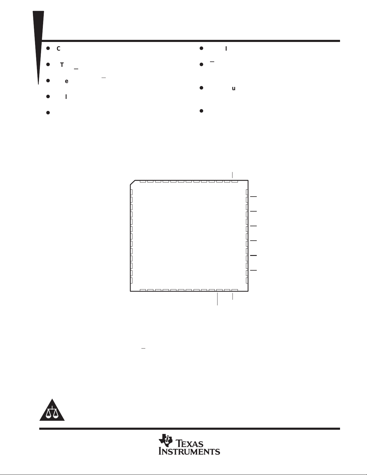
8-BIT TTL/BTL REGISTERED TRANSCEIVER
RC PACKAGE
(TOP VIEW)
SN74FB2033A
SCBS174J – NOVEMBER 1991 – REVISED SEPTEMBER 1999
D
High-Impedance State During Power Up
and Power Down
D
B-Port Biasing Network Preconditions the
Connector and PC Trace to the BTL
High-Level Voltage
D
TTL-Input Structures Incorporate Active
Clamping Networks to Aid in Line
Termination
D
Packaged in Plastic Quad Flatpack
description
GND
AO2
AI3
AO3
AI4
AO4
LOOPBACK
AI5
AO5
AI6
AO6
AI7
GND
CC
AI1
AO8
GND
GND
V
V
CC
CC
CLKAB/LEAB
IMODE1
IMODE0
BG V
CC
V
OMODE0
OMODE1
CLKBA/LEBA
OEA
OEB
AI2
AO1
52 51 50 49 48 47 46 45 44 43 42 41 40
1
2
3
4
5
6
7
8
9
10
11
12
13
14 15 16 17 18 19 20 21 22 23 24 25 26
AI8
AO7
CC
BG GND
B1
BIAS V
39
38
37
36
35
34
33
32
31
30
29
28
27
B8
OEB
GND
GND
B2
GND
B3
GND
B4
GND
B5
GND
B6
GND
B7
GND
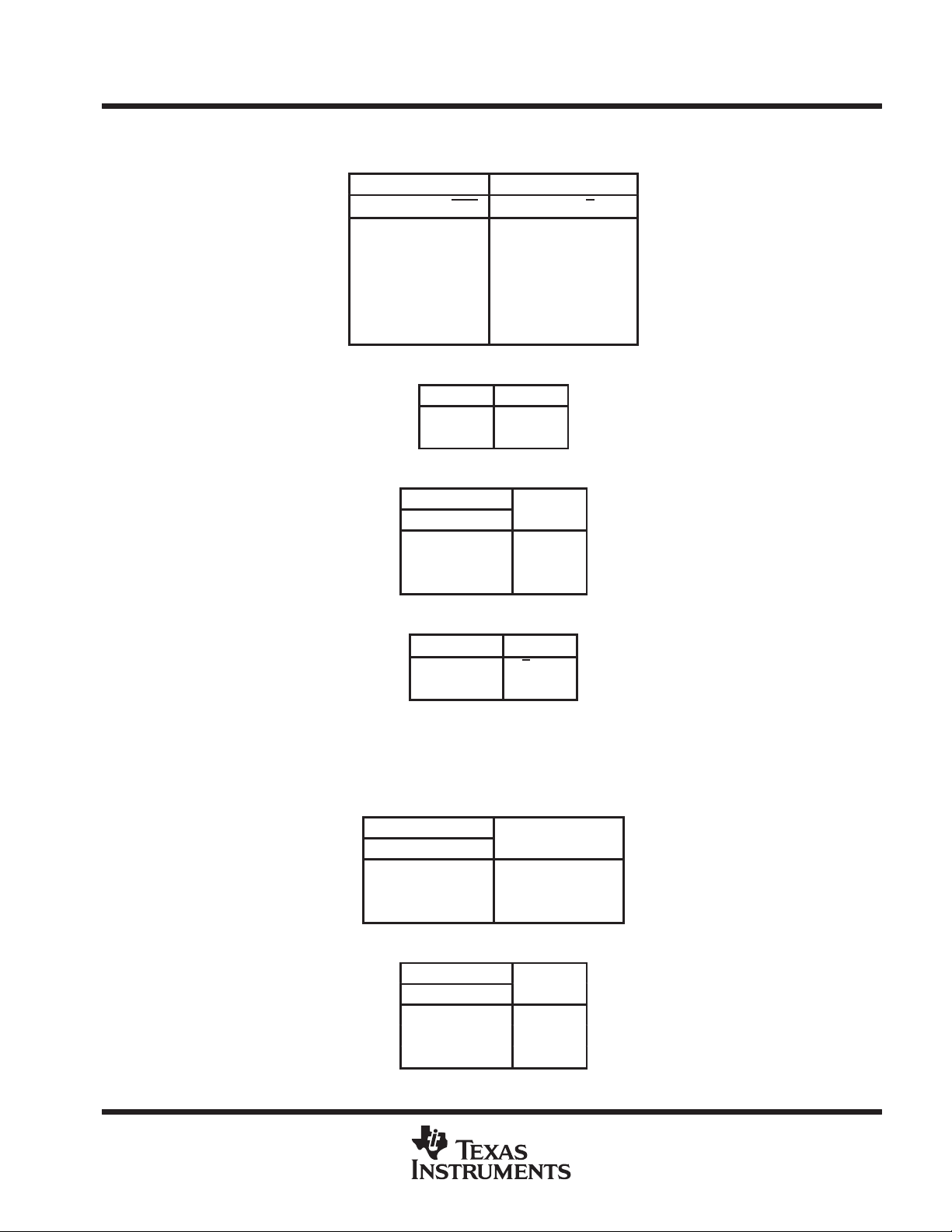
The SN74FB2033A is an 8-bit transceiver featuring a split input (AI) and output (AO) bus on the TTL-level A port.
The common-I/O, open-collector B port operates at backplane transceiver logic (BTL) signal levels.
The logic element for data flow in each direction is configured by two mode inputs (IMODE1 and IMODE0 for
B-to-A, OMODE1 and OMODE0 for A-to-B) as a buffer , a D-type flip-flop, or a D-type latch. When configured
in the buffer mode, the inverted input data appears at the output port. In the flip-flop mode, data is stored on
the rising edge of the appropriate clock input (CLKAB/LEAB or CLKBA/LEBA). In the latch mode, the clock
inputs serve as active-high transparent latch enables.
Please be aware that an important notice concerning availability, standard warranty, and use in critical applications of
Texas Instruments semiconductor products and disclaimers thereto appears at the end of this data sheet.
PRODUCTION DATA information is current as of publication date.
Products conform to specifications per the terms of Texas Instruments
standard warranty. Production processing does not necessarily include
testing of all parameters.
POST OFFICE BOX 655303 • DALLAS, TEXAS 75265
Copyright 1999, Texas Instruments Incorporated
1
SN74FB2033A
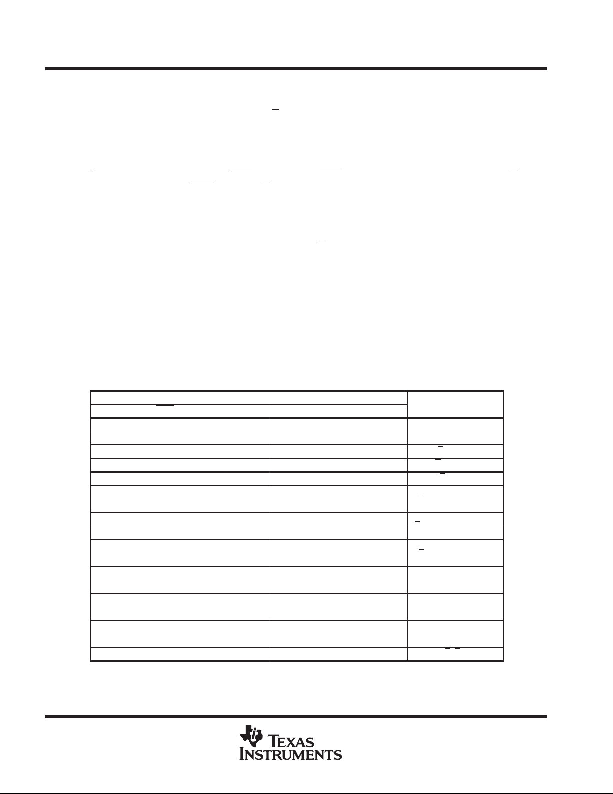
FUNCTION/MODE
Isolation
B
B
flip-fl
B
AI to AO, buffer mode
AI to AO, flip-flop mode
AI to AO, latch mode
8-BIT TTL/BTL REGISTERED TRANSCEIVER
SCBS174J – NOVEMBER 1991 – REVISED SEPTEMBER 1999
description (continued)
Data flow in the B-to-A direction, regardless of the logic element selected, is further controlled by the
LOOPBACK input. When LOOPBACK is low, B-port data is the B-to-A input. When LOOPBACK is high, the
output of the selected A-to-B logic element (prior to inversion) is the B-to-A input.
The AO port-enable/-disable control is provided by OEA. When OEA is low or when VCC is less than 2.5 V , the
AO port is in the high-impedance state. When OEA is high, the AO port is active (high or low logic levels).
The B port is controlled by OEB and OEB. If OEB is low, OEB is high, or VCC is less than 2.5 V, the B port is
inactive. If OEB is high and OEB is low, the B port is active.
BG VCC and BG GND are the bias-generator reference inputs.
The A-to-B and B-to-A logic elements are active, regardless of the state of their associated outputs. The logic
elements can enter new data (in flip-flop and latch modes) or retain previously stored data while the associated
outputs are in the high-impedance (AO port) or inactive (B port) states.
Output clamps are provided on the BTL outputs to reduce switching noise. One clamp reduces inductive ringing
effects on VOH during a low-to-high transition. The other clamps out ringing below the BTL VOL voltage of 0.75 V .
Both clamps are active only during ac switching and do not affect the BTL outputs during
steady-state conditions.
BIAS VCC establishes a voltage between 1.62 V and 2.1 V on the BTL outputs when VCC is not connected.
The SN74FB2033A is characterized for operation from 0°C to 70°C.
Function Tables
FUNCTION/MODE
INPUTS
OEA OEB OEB OMODE1 OMODE0 IMODE1 IMODE0 LOOPBACK
L L X X X X X X
L XH X X X X X
X H L L L X X X AI to B, buffer mode
X H L L H X X X AI to B, flip-flop mode
X H L H X X X X AI to B, latch mode
H L X X X L L L
H XH X X L L L
H L X X X L H L
H XH X X L H L
H L X X X H X L
H XH X X H X L
H L X X X L L H
H XH X X L L H
H L X X X L H H
H XH X X L H H
H L X X X H X H
H XH X X H X H
H H L X X X X L AI to B, B to AO
to AO, buffer mode
to AO,
to AO, latch mode
op mode
p
p
2
POST OFFICE BOX 655303 • DALLAS, TEXAS 75265
OUTPUT
OUTPUT
SN74FB2033A
8-BIT TTL/BTL REGISTERED TRANSCEIVER
SCBS174J – NOVEMBER 1991 – REVISED SEPTEMBER 1999
Function Tables (Continued)
ENABLE/DISABLE
INPUTS
OEA OEB OEB AO B
L X X Hi Z
H X X Active
X LL Inactive (H)
X LH Inactive (H)
X HL Active
X H H Inactive (H)
BUFFER
INPUT
L H
H L
LATCH
INPUTS
CLK/LE DATA
H L H
H HL
L X Q
OUTPUTS
OUTPUT
0
LOOPBACK
LOOPBACK
L B port
H Point P
†
Q is the input to the B-to-A
logic element.
‡
P is the output of the A-to-B
logic element (see functional
block diagram).
SELECT
INPUTS
MODE1 MODE0
L L Buffer
L H Flip-flop
H X Latch
FLIP-FLOP
INPUTS
CLK/LE DATA
L X Q
↑ LH
↑ H L
Q
SELECTED LOGIC
ELEMENT
†
‡
0
POST OFFICE BOX 655303 • DALLAS, TEXAS 75265
3
SN74FB2033A
8-BIT TTL/BTL REGISTERED TRANSCEIVER
SCBS174J – NOVEMBER 1991 – REVISED SEPTEMBER 1999
functional block diagram
23
OEB
24
OEB
AI1
21
20
47
Transceiver
1D
C1
50
1D
C1
OMODE1
OMODE0
CLKAB/LEAB
40
B1
P
IMODE1
IMODE0
CLKBA/LEBA
AO1
OEA
LOOPBACK
46
45
19
51
43
7
One of Eight Channels
Transceiver
1D
C1
Q
1D
C1
One of Eight Channels
4
POST OFFICE BOX 655303 • DALLAS, TEXAS 75265

VIHHigh-level input voltage
V
VILLow-level input voltage
V
IOLLow-level output current
mA
SN74FB2033A
8-BIT TTL/BTL REGISTERED TRANSCEIVER
SCBS174J – NOVEMBER 1991 – REVISED SEPTEMBER 1999
absolute maximum ratings over operating free-air temperature range (unless otherwise noted)
†
Supply voltage range, VCC –0.5 V to 7 V. . . . . . . . . . . . . . . . . . . . . . . . . . . . . . . . . . . . . . . . . . . . . . . . . . . . . . . . . .
Input clamp current, VI: Except B port –1.2V to 7V. . . . . . . . . . . . . . . . . . . . . . . . . . . . . . . . . . . . . . . . . . . . . . . . . .
B
port –1.2V to 3.5V. . . . . . . . . . . . . . . . . . . . . . . . . . . . . . . . . . . . . . . . . . . . . . . . . . . . . . .
Voltage range applied to any B output in the disabled or power-off state, VO –0.5 V to 3.5 V. . . . . . . . . . . . . .
Voltage range applied to any output in the high state, VO: A port –0.5 V to V
. . . . . . . . . . . . . . . . . . . . . . . .
CC
Input clamp current, IIK: Except B port –40 mA. . . . . . . . . . . . . . . . . . . . . . . . . . . . . . . . . . . . . . . . . . . . . . . . . . . .
B port –18 mA. . . . . . . . . . . . . . . . . . . . . . . . . . . . . . . . . . . . . . . . . . . . . . . . . . . . . . . . . . .
Current applied to any single output in the low state, I
Package thermal impedance, θ
Storage temperature range, T
†
Stresses beyond those listed under “absolute maximum ratings” may cause permanent damage to the device. These are stress ratings only, and
functional operation of the device at these or any other conditions beyond those indicated under “recommended operating conditions” is not
implied. Exposure to absolute-maximum-rated conditions for extended periods may affect device reliability.
NOTE 1: The package thermal impedance is calculated in accordance with JESD 51.
(see Note 1) 44°C/W. . . . . . . . . . . . . . . . . . . . . . . . . . . . . . . . . . . . . . . . . . . . .
JA
–65°C to 150°C. . . . . . . . . . . . . . . . . . . . . . . . . . . . . . . . . . . . . . . . . . . . . . . . . . .
stg
: A port 48 mA. . . . . . . . . . . . . . . . . . . . . . . . . . . . . . . . .
O
recommended operating conditions (see Note 2)
MIN NOM MAX UNIT
VCC, BG V
BIAS V
CC
I
OH
∆t/∆v Input transition rise or fall rate Except B port 10 ns/V
T
A
NOTE 2: All unused inputs of the device must be held at VCC or GND to ensure proper device operation. Refer to the TI application report,
Implications of Slow or Floating CMOS Inputs
Supply voltage 4.75 5 5.25 V
CC
Supply voltage 4.5 5 5.5 V
p
p
High-level output current AO port –3 mA
p
Operating free-air temperature 0 70 °C
, literature number SCBA004.
B port 1.62 2.3
Except B port 2
B port 0.75 1.47
Except B port 0.8
AO port 24
B port 100
POST OFFICE BOX 655303 • DALLAS, TEXAS 75265
5

SN74FB2033A
V
4.75 V
AO port
V
4.75 V
V
V
B
V
V
I
A
I
A
C
B ort
pF
I
(BIAS VCC)
V
0 to 2 V
V
(BIAS VCC)
V
A
8-BIT TTL/BTL REGISTERED TRANSCEIVER
SCBS174J – NOVEMBER 1991 – REVISED SEPTEMBER 1999
electrical characteristics over recommended operating free-air temperature range (unless
otherwise noted)
PARAMETER TEST CONDITIONS MIN TYP
V
IK
V
I
I
IH
IL
I
OH
I
OZPU
I
OZPD
I
OZH
I
OZL
I
OS
I
CC
C
C
†
All typical values are at VCC = 5 V.
‡
For I/O ports, the parameters IIH and IIL include the off-state output current.
§
Not more than one output should be shorted at a time, and the duration of the short circuit should not exceed one second.
AO port
OH
p
OL
port
Except B port VCC = 0, VI = 5.25 V 100 µA
Except B port VCC = 5.25 V, VI = 2.7 V 50
‡
B port
Except B port VCC = 5.25 V, VI = 0.5 V –50
‡
B port
B port VCC = 0 to 5.25 V, VO = 2.1 V 100 µA
AO port VCC = 5.25 V, VO = 2.7 V 50 µA
AO port VCC = 5.25 V, VO = 0.5 V –50 µA
§
AO port VCC = 5.25 V, VO = 0 –40 –80 –150 mA
All outputs on VCC = 5.25 V, IO = 0 45 70 mA
AI port and
i
control inputs
AO port VO = 0.5 V or 2.5 V 5 pF
o
B port
io
per IEEE Std 1194.1-1991
VCC = 4.75 V II = –18 mA –1.2 V
VCC = 4.75 V to 5.25 V IOH = –10 µA VCC–1.1
=
CC
=
CC
= 4.75
CC
VCC = 0 to 5.25 V, VI = 2.1 V 100
VCC = 5.25 V, VI = 0.75 V –100
VCC = 0 to 2.1 V, VO = 0.5 V to 2.7 V 50 µA
VCC = 2.1 V to 0, VO = 0.5 V to 2.7 V –50 µA
VI = 0.5 V or 2.5 V 5 pF
VCC = 0 to 4.75 V 6
VCC = 4.75 V to 5.25 V 6
IOH = –3 mA 2.5 2.85 3.4
IOH = –32 mA 2
IOL = 20 mA 0.33 0.5
IOL = 55 mA 0.8
IOL = 100 mA 0.75 1.1
IOL = 4 mA 0.5
†
MAX UNIT
V
µ
µ
p
live-insertion characteristics over recommended operating free-air temperature range (see Note 3)
PARAMETER TEST CONDITIONS MIN MAX UNIT
CC
V
I
O
NOTE 3: The power-up sequence is: GND, BIAS VCC, VCC.
6
B port VCC = 0, VI (BIAS VCC) = 4.5 V to 5.5 V 1.62 2.1 V
O
B port
VCC = 0 to 4.5 V
VCC = 4.5 V to 5.5 V
VCC = 0, VB = 1 V, Vl (BIAS VCC) = 4.5 V to 5.5 V –1
VCC = 0 to 5.5 V, OEB = 0 to 0.8 V 100
VCC = 0 to 2.2 V, OEB = 0 to 5 V 100
POST OFFICE BOX 655303 • DALLAS, TEXAS 75265
=
B
,
l
= 4.5 V to 5.5
10
10
µ
µA

SN74FB2033A
8-BIT TTL/BTL REGISTERED TRANSCEIVER
SCBS174J – NOVEMBER 1991 – REVISED SEPTEMBER 1999
timing requirements over recommended ranges of supply voltage and operating free-air
temperature (unless otherwise noted) (see Figure 2)
VCC = 5 V,
f
clock
t
w
t
su
t
h
TA = 25°C
MIN MAX
Clock frequency 150 150 MHz
Pulse duration CLKAB/LEAB or CLKBA/LEBA 3.3 3.3 ns
Setup time Data before CLKAB/LEAB or CLKBA/LEBA↑ 2.7 2.7 ns
Hold time Data after CLKAB/LEAB or CLKBA/LEBA↑ 0.7 0.7 ns
MIN MAX UNIT
POST OFFICE BOX 655303 • DALLAS, TEXAS 75265
7

SN74FB2033A
(INPUT)
(OUTPUT)
B
ns
B
AO
ns
B
ns
B
AO
ns
OEB
B
ns
OEB
B
ns
OEA
AO
ns
OEA
AO
ns
CLKAB/LEAB
B
ns
CLKBA/LEBA
AO
ns
OMODE
B
ns
IMODE
AO
ns
LOOPBACK
AO
ns
AI
AO
ns
ns
ns
8-BIT TTL/BTL REGISTERED TRANSCEIVER
SCBS174J – NOVEMBER 1991 – REVISED SEPTEMBER 1999
switching characteristics over recommended ranges of supply voltage and operating free-air
temperature (unless otherwise noted) (see Figure 2)
PARAMETER
f
max
t
PLH
t
PHL
t
PLH
t
PHL
t
PLH
t
PHL
t
PLH
t
PHL
t
PLH
t
PHL
t
PLH
t
PHL
t
PZH
t
PZL
t
PHZ
t
PLZ
t
PLH
t
PHL
t
PLH
t
PHL
t
PLH
t
PHL
t
PLH
t
PHL
t
PLH
t
PHL
t
PLH
t
PHL
t
r
t
f
t
r
t
f
B-port input pulse rejection 1 ns
Rise time,1.3 V to 1.8 V, B port 0.5 1.2 2.1 0.5 3
Fall time, 1.8 V to 1.3 V, B port 0.5 1.4 2.3 0.5 3
Rise time, 10% to 90%, AO 2 3.3 4.2 2 5
Fall time, 90% to 10%, AO 1 2.5 3.4 1 5
FROM
AI
(through mode)
B
(through mode)
AI
(transparent)
B
(transparent)
TO
VCC = 5 V,
TA = 25°C
MIN TYP MAX
150 150 MHz
2.3 3.6 4.6 2.3 5.6
1.9 3 4.2 1.9 4.5
2.5 4.2 5.5 2.5 6.1
3 4.2 5.6 3 5.7
2.3 3.6 4.6 2.3 5.6
1.9 3 4.1 1.9 4.5
2.5 4.2 5.5 2.5 6.1
3 4.2 5.6 3 5.7
2.4 3.7 4.7 2.4 5.8
1.8 3 4.1 1.8 4.4
2 3.4 4.3 2 5.2
2 3.3 4.4 2 4.8
2 3.5 4.6 2 5.1
2.7 4.2 5.1 2.7 5.4
2.1 4 5 2.1 5.5
1.6 2.8 3.9 1.6 4.3
3 4.7 5.8 3 6.9
2.8 4.3 5.6 2.8 6.1
2 3.6 4.9 2 5.4
2.2 3.5 4.7 2.2 5.1
2.4 5 6.1 2.4 7.2
2.4 4.5 6 2.4 6.7
1.8 4 5.3 1.8 5.9
2.3 4.1 5.2 2.3 5.4
2.4 5 7 2.4 8
3.1 4.6 5.7 3.1 5.9
1.9 3.7 5.5 1.9 6.1
2.6 4.2 5.6 2.6 5.8
MIN MAX UNIT
output-voltage characteristics
V
OHP
V
OHV
V
OLV
8
Peak output voltage during turnoff of 100 mA into 40 nH B port See Figure 1 4.5 V
Minimum output voltage during turnoff of 100 mA into 40 nH
Minimum output voltage during high-to-low switch B port IOL = –50 mA 0.3 V
PARAMETER
POST OFFICE BOX 655303 • DALLAS, TEXAS 75265
B port
TEST
CONDITIONS
See Figure 1 1.62 V
MIN MAX UNIT

SN74FB2033A
8-BIT TTL/BTL REGISTERED TRANSCEIVER
SCBS174J – NOVEMBER 1991 – REVISED SEPTEMBER 1999
PARAMETER MEASUREMENT INFORMATION
2.1 V
From Output
Under Test
40 nH
Figure 1. Load Circuit for V
OHP
9 Ω
30 pF
and V
OHV
POST OFFICE BOX 655303 • DALLAS, TEXAS 75265
9

SN74FB2033A
8-BIT TTL/BTL REGISTERED TRANSCEIVER
SCBS174J – NOVEMBER 1991 – REVISED SEPTEMBER 1999
PARAMETER MEASUREMENT INFORMATION
2.1 V
From Output
Under Test
CL = 50 pF
(see Note A)
LOAD CIRCUIT FOR A OUTPUTS
Timing Input
Data Input
VOLTAGE WAVEFORMS
SETUP AND HOLD TIMES
Input 1.5 V 1.5 V
Output
VOLTAGE WAVEFORMS
PROPAGATION DELAY TIMES (A TO B)
Input
500 Ω
500 Ω
t
su
1.5 V 1.5 V
t
PHL
1.5 V
t
h
7 V
S1
1.55 V1.55 V
1.55 V1.55 V
t
PLH
Open
3 V
0 V
3 V
0 V
3 V
0 V
V
V
2.1 V
1 V
From Output
Under Test
CL = 30 pF
(see Note A)
LOAD CIRCUIT FOR B OUTPUTS
Output
Control
Output
Waveform 1
S1 at 7 V
(see Note B)
OH
OL
Output
Waveform 2
S1 at Open
(see Note B)
ENABLE AND DISABLE TIMES (A PORT)
9 Ω
Test
Point
1.5 V 1.5 VInput
VOLTAGE WAVEFORMS
PULSE DURATION
1.5 V 1.5 V
t
PZL
1.5 V
t
PZH
1.5 V
VOLTAGE WAVEFORMS
TEST S1
t
PLH/tPHL
t
PLZ/tPZL
t
PHZ/tPZH
t
w
Open
7 V
Open
t
PLZ
VOL + 0.3 V
t
PHZ
VOH – 0.3 V
3 V
0 V
3 V
0 V
3.5 V
V
OL
V
OH
≈ 0 V
t
PHL
Output
VOLTAGE WAVEFORMS
PROPAGATION DELAY TIMES (B TO A)
NOTES: A. CL includes probe and jig capacitance.
B. Waveform 1 is for an output with internal conditions such that the output is low except when disabled by the output control.
Waveform 2 is for an output with internal conditions such that the output is high except when disabled by the output control.
C. All input pulses are supplied by generators having the following characteristics: TTL inputs: PRR ≤ 10 MHz, ZO = 50 Ω, tr ≤ 2.5 ns,
tf≤ 2.5 ns; BTL inputs: PRR ≤ 10 MHz, ZO = 50 Ω, tr ≤ 2.5 ns, tf≤ 2.5 ns.
D. The outputs are measured one at a time with one transition per measurement.
1.5 V 1.5 V
Figure 2. Load Circuits and Voltage Waveforms
10
POST OFFICE BOX 655303 • DALLAS, TEXAS 75265
t
PLH
V
OHP
V
OH
V
OL
VOLTAGE WAVEFORMS
V
OHV
2.1 V
V
1 V
OLV

IMPORTANT NOTICE
T exas Instruments and its subsidiaries (TI) reserve the right to make changes to their products or to discontinue
any product or service without notice, and advise customers to obtain the latest version of relevant information
to verify, before placing orders, that information being relied on is current and complete. All products are sold
subject to the terms and conditions of sale supplied at the time of order acknowledgement, including those
pertaining to warranty, patent infringement, and limitation of liability.
TI warrants performance of its semiconductor products to the specifications applicable at the time of sale in
accordance with TI’s standard warranty. Testing and other quality control techniques are utilized to the extent
TI deems necessary to support this warranty . Specific testing of all parameters of each device is not necessarily
performed, except those mandated by government requirements.
CERTAIN APPLICATIONS USING SEMICONDUCTOR PRODUCTS MAY INVOLVE POTENTIAL RISKS OF
DEATH, PERSONAL INJURY, OR SEVERE PROPERTY OR ENVIRONMENTAL DAMAGE (“CRITICAL
APPLICATIONS”). TI SEMICONDUCTOR PRODUCTS ARE NOT DESIGNED, AUTHORIZED, OR
WARRANTED TO BE SUITABLE FOR USE IN LIFE-SUPPORT DEVICES OR SYSTEMS OR OTHER
CRITICAL APPLICA TIONS. INCLUSION OF TI PRODUCTS IN SUCH APPLICATIONS IS UNDERST OOD TO
BE FULLY AT THE CUSTOMER’S RISK.
In order to minimize risks associated with the customer’s applications, adequate design and operating
safeguards must be provided by the customer to minimize inherent or procedural hazards.
TI assumes no liability for applications assistance or customer product design. TI does not warrant or represent
that any license, either express or implied, is granted under any patent right, copyright, mask work right, or other
intellectual property right of TI covering or relating to any combination, machine, or process in which such
semiconductor products or services might be or are used. TI’s publication of information regarding any third
party’s products or services does not constitute TI’s approval, warranty or endorsement thereof.
Copyright 1999, Texas Instruments Incorporated
 Loading...