

D
Compatible With IEEE Std 1 194.1-1991
(BTL)
D
TTL A Port, Backplane Transceiver Logic
(BTL) B Port
D
Open-Collector B-Port Outputs Sink
100 mA
D
Isolated Logic-Ground and Bus-Ground
Pins Reduce Noise
D
High-Impedance State During Power Up
and Power Down
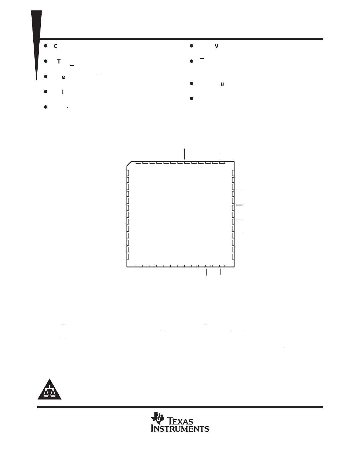
SN74FB2031
9-BIT TTL/BTL ADDRESS/DATA TRANSCEIVER
SCBS176K – NOVEMBER 1991 – REVISED SEPTEMBER 1999
D
BIAS VCC Minimizes Signal Distortion
During Live Insertion or Withdrawal
D
B-Port Biasing Network Preconditions the
Connector and PC Trace to the BTL
High-Level Voltage
D
TTL-Input Structures Incorporate Active
Clamping to Aid in Line Termination
D
Packaged in Plastic Quad Flatpack
RC PACKAGE
(TOP VIEW)
CC
GND
A3
GND
A4
GND
A5
GND
A6
GND
A7
GND
A8
GND
GND
A1
LCB
SEL1
CC
V
CC
LCA
BG V
OEA
BIAS V
BG GND
OEB
SEL0
A2
52 51 50 49 48 47 46 45 44 43 42 41 40
1
2
3
4
5
6
7
8
9
10
11
12
13
14 15 16 17 18 19 20 21 22 23 24 25 26
A9
OEB
TDO
TCK
TDI
V
V
CC
CC
TMS
B9
GND
GND
B1
39
38
37
36
35
34
33
32
31
30
29
28
27
B8
GND
B2
GND
B3
GND
B4
GND
B5
GND
B6
GND
B7
GND
description
The SN74FB2031 device is a 9-bit transceiver designed to translate signals between TTL and backplane
transceiver logic (BTL) environments. It is specifically designed to be compatible with IEEE Std 1 194.1-1991.
The B port operates at BTL-signal levels. The open-collector B ports are specified to sink 100 mA. Two output
enables (OEB and OEB) are provided for the B outputs. When OEB is low, OEB is high, or VCC is less than 2.1 V ,
the B
port is turned off.
The A port operates at TTL signal levels. The A outputs reflect the inverse of the data at the B
port when the
A-port output enable (OEA) is high. When OEA is low or VCC is less than 2.1 V, the A outputs are in the
high-impedance state.
Please be aware that an important notice concerning availability, standard warranty, and use in critical applications of
Texas Instruments semiconductor products and disclaimers thereto appears at the end of this data sheet.
PRODUCTION DATA information is current as of publication date.
Products conform to specifications per the terms of Texas Instruments
standard warranty. Production processing does not necessarily include
testing of all parameters.
POST OFFICE BOX 655303 • DALLAS, TEXAS 75265
Copyright 1999, Texas Instruments Incorporated
1
SN74FB2031
FUNCTION
B d
Isolation
9-BIT TTL/BTL ADDRESS/DATA TRANSCEIVER
SCBS176K – NOVEMBER 1991 – REVISED SEPTEMBER 1999
description (continued)
Pins are allocated for the 4-wire IEEE Std 1149.1 (JT AG) test bus. TMS and TCK are not connected and TDI
is shorted to TDO.
BIAS VCC establishes a voltage between 1.62 V and 2.1 V on the BTL outputs when VCC is not connected.
BG VCC and BG GND are the supply inputs for the bias generator.
The SN74FB2031 is characterized for operation from 0°C to 70°C.
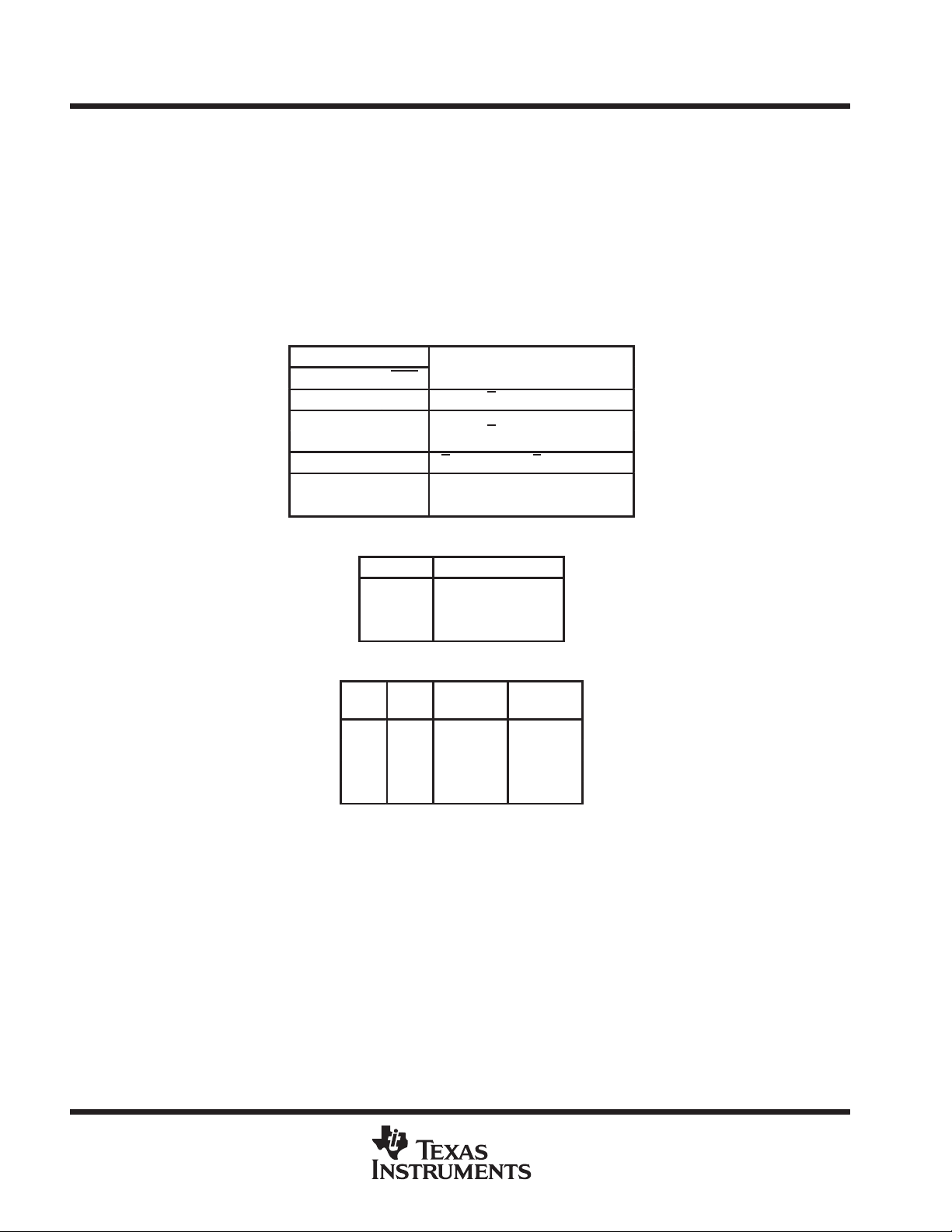
Function Tables
TRANSCEIVER
INPUTS
OEA OEB OEB
L H L A data to B bus
H L X
H XH
H H L A data to B bus, B data to A bus
L L X
L X H
ata to A bus
STORAGE MODE
SELECT
MUX
A→B
RESULT
MUX
B→A
LCA, LCB
0 Transparent
1 Latches latched
↑ Flip-flops triggered
SEL0
SEL1
0 0 Latch Latch
0 1 Through Through
1 0 Flip-flop Flip-flop
1 1 Flip-flop Latch
2
POST OFFICE BOX 655303 • DALLAS, TEXAS 75265
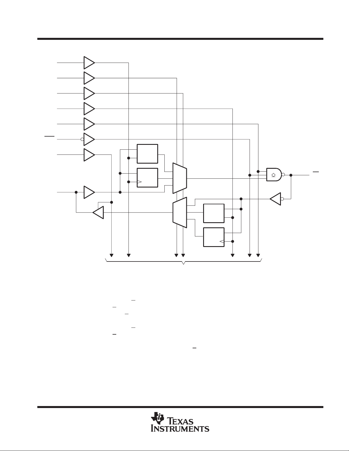
functional block diagram
18
LCA
SN74FB2031
9-BIT TTL/BTL ADDRESS/DATA TRANSCEIVER
SCBS176K – NOVEMBER 1991 – REVISED SEPTEMBER 1999
SEL0
SEL1
LCB
OEB
OEB
OEA
A1
20
15
16
46
45
47
50
1D
C1
1D
C1
MUX
MUX
C1
1D
C1
1D
40
B1
To Eight Other Channels
absolute maximum ratings over operating free-air temperature range (unless otherwise noted)
Supply voltage range, VCC –0.5 V to 7 V. . . . . . . . . . . . . . . . . . . . . . . . . . . . . . . . . . . . . . . . . . . . . . . . . . . . . . . . . .
Input voltage range, VI: Except B port –1.2 V to 7 V. . . . . . . . . . . . . . . . . . . . . . . . . . . . . . . . . . . . . . . . . . . . . . . .
B
port –1.2 V to 3.5 V. . . . . . . . . . . . . . . . . . . . . . . . . . . . . . . . . . . . . . . . . . . . . . . . . . . . . .
Voltage range applied to any B output in the disabled or power-off state, VO –0.5 V to 3.5 V. . . . . . . . . . . . . .
Voltage range applied to any output in the high state, VO –0.5 V to V
Input clamp current, IIK: Except B port –40 mA. . . . . . . . . . . . . . . . . . . . . . . . . . . . . . . . . . . . . . . . . . . . . . . . . . . . .
B port –18 mA. . . . . . . . . . . . . . . . . . . . . . . . . . . . . . . . . . . . . . . . . . . . . . . . . . . . . . . . . . . .
Current applied to any single output in the low state, I
Package thermal impedance, θ
Storage temperature range, T
†
Stresses beyond those listed under “absolute maximum ratings” may cause permanent damage to the device. These are stress ratings only, and
functional operation of the device at these or any other conditions beyond those indicated under “recommended operating conditions” is not
implied. Exposure to absolute-maximum-rated conditions for extended periods may affect device reliability.
NOTE 1: The package thermal impedance is calculated in accordance with JESD 51.
(see Note 1) 44°C/W. . . . . . . . . . . . . . . . . . . . . . . . . . . . . . . . . . . . . . . . . . . . .
JA
–65°C to 150°C. . . . . . . . . . . . . . . . . . . . . . . . . . . . . . . . . . . . . . . . . . . . . . . . . . .
stg
. . . . . . . . . . . . . . . . . . . . . . . . . . . . . . .
: A port 48 mA. . . . . . . . . . . . . . . . . . . . . . . . . . . . . . . . .
O
B port 200 mA. . . . . . . . . . . . . . . . . . . . . . . . . . . . . . . .
†
CC
POST OFFICE BOX 655303 • DALLAS, TEXAS 75265
3
 Loading...