

D
Compatible With IEEE Std 1 194.1-1991
(BTL)
D
LVTTL A Port, Backplane Transceiver Logic
(BTL) B Port
D
Open-Collector B-Port Outputs Sink
100 mA
D
B-Port Biasing Network Preconditions the
Connector and PC Trace to the BTL
High-Level Voltage
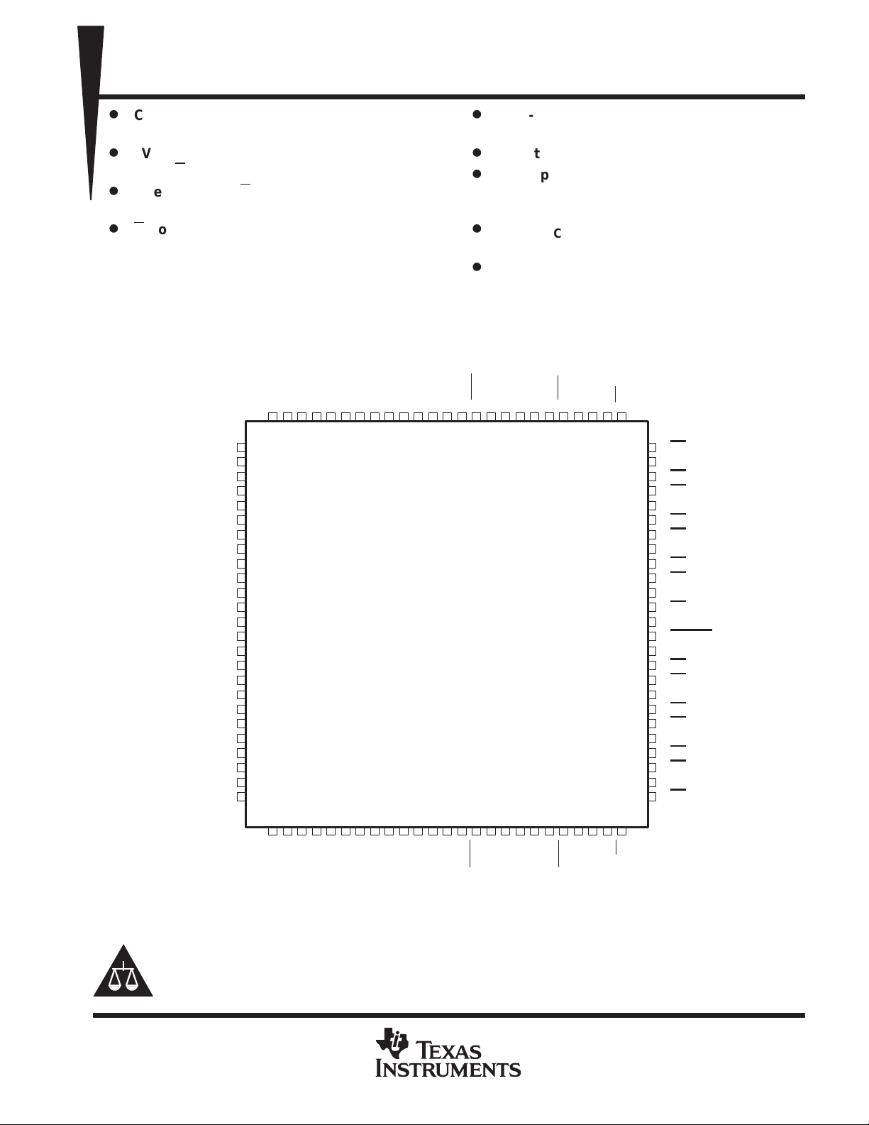
SN74FB1653
17-BIT LVTTL/BTL UNIVERSAL STORAGE TRANSCEIVER
WITH BUFFERED CLOCK LINE
SCBS702C – AUGUST 1997 – REVISED SEPTEMBER 1999
D
High-Impedance State During Power Up
and Power Down
D
Selectable Clock Delay
D
TTL-Input Structures Incorporate Active
Clamping Networks to Aid in Line
Termination
D
BIAS VCC Minimizes Signal Distortion
During Live Insertion/Withdrawal
D
Packaged in Plastic High-Power
Low-Profile Quad Flatpack
PCA PACKAGE
(TOP VIEW)
VCC(3.3 V)
V
(5 V)
CC
GND
1AO6
1AI6
1AO7
1AI7
GND
1AO8
1AI8
1AO9
1AI9
GND
2CLK
(3.3 V)
V
CC
2AO2
2AI2
GND
2AO3
2AI3
2AO4
2AI4
GND
(5 V)
V
CC
(3.3 V)
V
CC
1
2
3
4
5
6
7
8
9
10
11
12
13
14
15
16
17
18
19
20
21
22
23
24
25
1AI5
1AO5
99
100
27
26
1AI4
98
28
1AO4
GND
96
97
30
29
1AI3
1AO3
94
95
32
31
1AI2
93
33
GND
1AO2
91
92
35
34
1AI1
1AO12AI9
89
90
37
36
(5 V)
CC
V
1OEA
87
88
39
38
1OEA
1LEBA
85
86
41
40
1CLKAB
1LEAB
1CLKBA
82
83
84
44
43
42
1OEB
1OEB
80
81
46
45
CC
REF
BG GND/GND
BG V
V
77
78
79
49
48
47
1B1
76
75
74
73
72
71
70
69
68
67
66
65
64
63
62
61
60
59
58
57
56
55
54
53
52
51
50
1B2
GND
1B3
1B4
GND
1B5
1B6
GND
1B7
1B8
GND
1B9
2SEL2
2CLKAB
GND
2B2
2B3
GND
2B4
2B5
GND
2B6
2B7
GND
2B8
2AI5
2AO5
Please be aware that an important notice concerning availability, standard warranty, and use in critical applications of
Texas Instruments semiconductor products and disclaimers thereto appears at the end of this data sheet.
PRODUCTION DATA information is current as of publication date.
Products conform to specifications per the terms of Texas Instruments
standard warranty. Production processing does not necessarily include
testing of all parameters.
2AI6
2AO6
2AI8
2AI7
GND
2AO7
POST OFFICE BOX 655303 • DALLAS, TEXAS 75265
2AO8
GND
2AO9
(5 V)
2OEA
CC
V
2OEA
2LEBA
2CLKBA
2CLKAB
2OEB
2LEAB
CC
2B9
GND
2OEB
2SEL1
BIAS V
Copyright 1999, Texas Instruments Incorporated
1
SN74FB1653
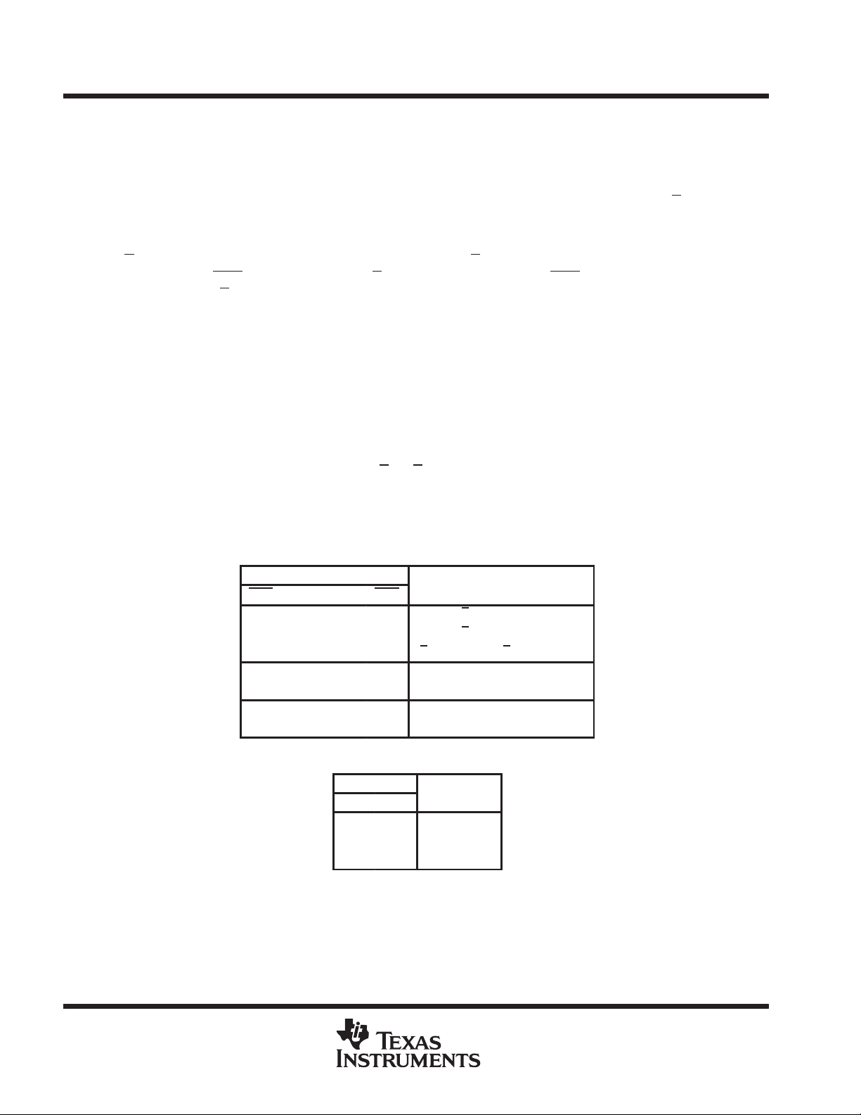
FUNCTION
B-bus isolation
A-bus isolation
FUNCTION
17-BIT LVTTL/BTL UNIVERSAL STORAGE TRANSCEIVER
WITH BUFFERED CLOCK LINE
SCBS702C – AUGUST 1997 – REVISED SEPTEMBER 1999
description
The SN74FB1653 device contains an 8-bit and a 9-bit transceiver with a buffered clock. The clock and
transceivers are designed to translate signals between L VTTL and BTL environments. It is specifically designed
to be compatible with IEEE Std 1194.1-1991 (BTL).
The A port operates at L VTTL signal levels. The A outputs reflect the inverse of the data at the B port when the
A-port output enable (OEA) is high. When OEA is low or when V
are in the high-impedance state.
port operates at BTL signal levels. The open-collector B ports are specified to sink 100 mA. Two output
The B
enables (OEB and OEB
) are provided for the B outputs. When OEB is low, OEB is high, or VCC(5 V) is typically
less than 2.5 V, the B port is turned off.
The clock-select inputs (2SEL1 and 2SEL2) are used to configure the TTL-to-BTL clock paths and delays. Refer
to the
Mux-Mode Delay
table.
(5 V) is typically less than 2.5 V , the A outputs
CC
BIAS V
establishes a voltage between 1.62 V and 2.1 V on the BTL outputs when VCC(5 V) is not connected.
CC
BG VCC and BG GND are the supply inputs for the bias generator.
V
is used to bypass the internal threshold reference voltage of the device. It is recommended that this pin
REF
be decoupled with a 0.1-µF capacitor.
Enhanced heat-dissipation techniques should be used when operating this device from: (a) AI to A0 at
frequencies greater than 50 MHz, or (b) AI to B, or B to A0 at frequencies greater than 100 MHz.
The SN74FB1653 is characterized for operation from 0°C to 70°C.
Function Tables
TRANSCEIVER
INPUTS
OEA OEA OEB OEB
X X H L A data to B bus
L HXX B data to A bus
L HHLA data to B bus, B data to A bus
X X L X
X XXH
H X X X
X L X X
STORAGE MODE
INPUTS
LE CLK
H X Transparent
L ↑ Store data
L L Storage
2
POST OFFICE BOX 655303 • DALLAS, TEXAS 75265
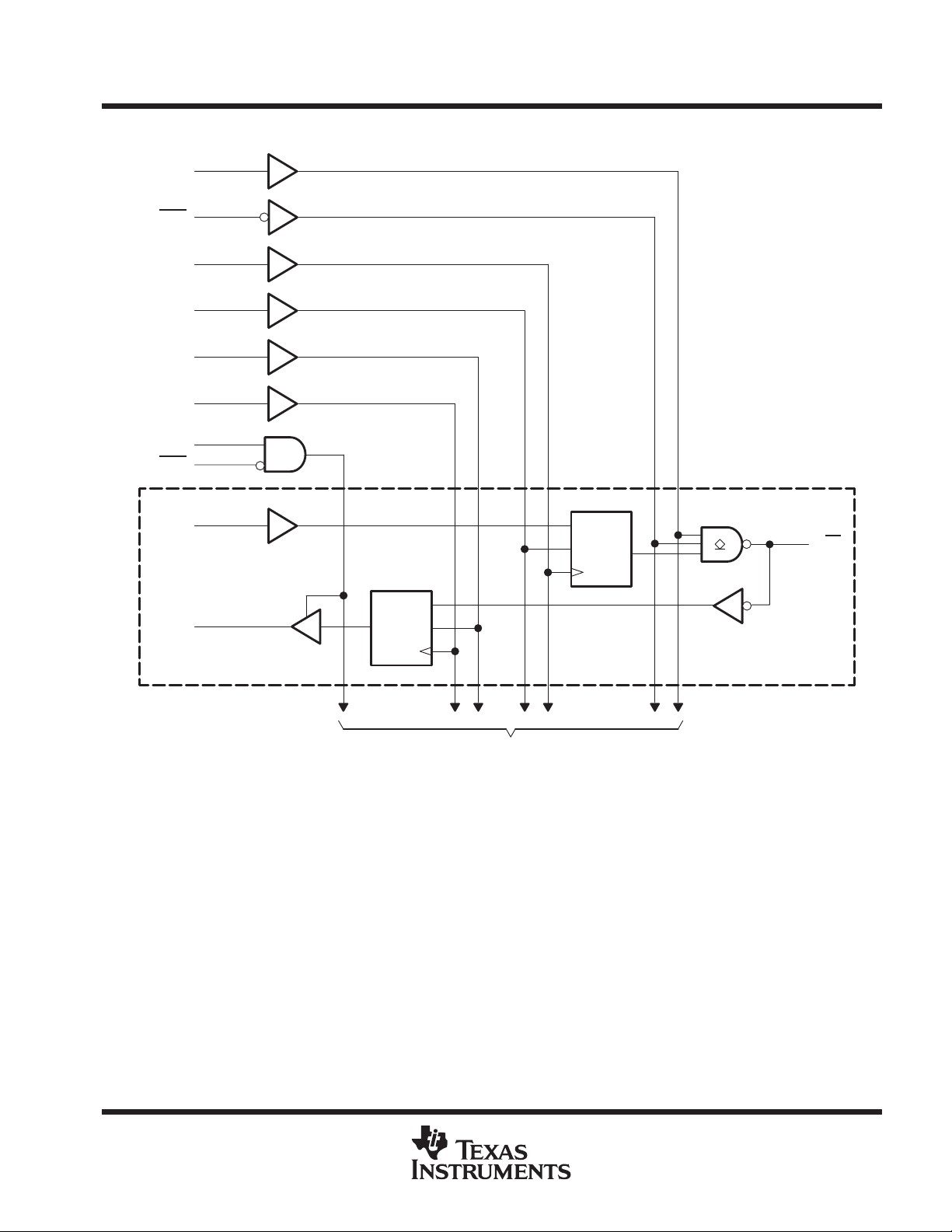
functional block diagram
SN74FB1653
17-BIT LVTTL/BTL UNIVERSAL STORAGE TRANSCEIVER
WITH BUFFERED CLOCK LINE
SCBS702C – AUGUST 1997 – REVISED SEPTEMBER 1999
1OEB
1OEB
1CLKAB
1LEAB
1LEBA
1CLKBA
1OEA
1OEA
1AI1
1AO1
81
80
83
82
85
84
87
86
90
89
C1
1D
C2
1D
C2
C1
76
1B1
To Eight Other Channels
POST OFFICE BOX 655303 • DALLAS, TEXAS 75265
3
 Loading...