

SN74F161A
SYNCHRONOUS 4-BIT BINARY COUNTER
SDFS056A – D2932, MARCH 1987 – REVISED OCTOBER 1993
• Internal Look-Ahead Circuitry for Fast
Counting
• Carry Output for N-Bit Cascading
• Fully Synchronous Operation for Counting
• Package Options Include Plastic
Small-Outline Packages and Standard
Plastic 300-mil DIPs
description
This synchronous, presettable, 4-bit binary
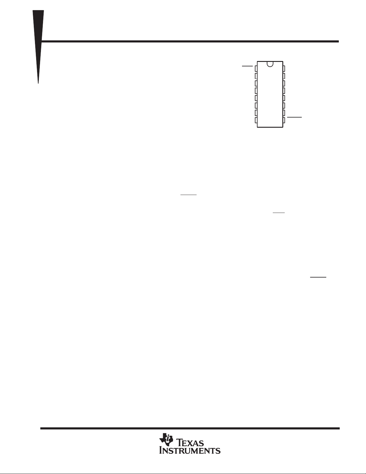
D OR N PACKAGE
(TOP VIEW)
CLR
CLK
ENP
GND
1
2
3
A
4
B
5
C
6
D
7
8
16
15
14
13
12
11
10
9
V
CC
RCO
Q
A
Q
B
Q
C
Q
D
ENT
LOAD
counter features an internal carry look-ahead
circuitry for application in high-speed counting
designs. Synchronous operation is provided by
having all flip-flops clocked simultaneously so that the outputs change coincident with each other when so
instructed by the count-enable (ENP, ENT) inputs and internal gating. This mode of operation eliminates the
output counting spikes that are normally associated with asynchronous (ripple-clock) counters; however,
counting spikes may occur on the ripple-carry (RCO) output. A buffered clock (CLK) input triggers the four
flip-flops on the rising (positive-going) edge of the clock input waveform.
This counter is fully programmable; that is, it may be preset to any number between 0 and 15. As presetting is
synchronous, setting up a low level at the load (LOAD
) input disables the counter and causes the outputs to
agree with the setup data after the next clock pulse regardless of the levels of the enable inputs.
The clear function for the SN74F161A is asynchronous and a low level at the clear (CLR
) input sets all four of
the flip-flop outputs low regardless of the levels of the clock, load, or enable inputs.
The carry look-ahead circuitry provides for cascading counters for n-bit synchronous applications without
additional gating. Instrumental in accomplishing this function are two count-enable (ENP, ENT) inputs and a
ripple-carry (RCO) output. Both ENP and ENT must be high to count, and ENT if fed forward to enable RCO.
RCO thus enabled will produce a high-level pulse while the count is 15 (HHHH). The high-level overflow
ripple-carry pulse can be used to enable successive cascaded stages. Transitions at ENP or ENT are allowed
regardless of the level of the clock input.
The SN74F161A features a fully independent clock circuit. Changes at control inputs (ENP , ENT, or LOAD
) that
will modify the operating mode have no effect on the contents of the counter until clocking occurs. The function
of the counter (whether enabled, disabled, loading, or counting) will be dictated solely by the conditions meeting
the setup and hold times.
The SN74F161A is characterized for operation from 0°C to 70°C.
PRODUCTION DATA information is current as of publication date.
Products conform to specifications per the terms of Texas Instruments
standard warranty. Production processing does not necessarily include
testing of all parameters.
POST OFFICE BOX 655303 • DALLAS, TEXAS 75265
Copyright 1993, Texas Instruments Incorporated
2–1
SN74F161A
SYNCHRONOUS 4-BIT BINARY COUNTER
SDFS056A – D2932, MARCH 1987 – REVISED OCT OBER 1993
1
9
10
7
2
3
4
5
6
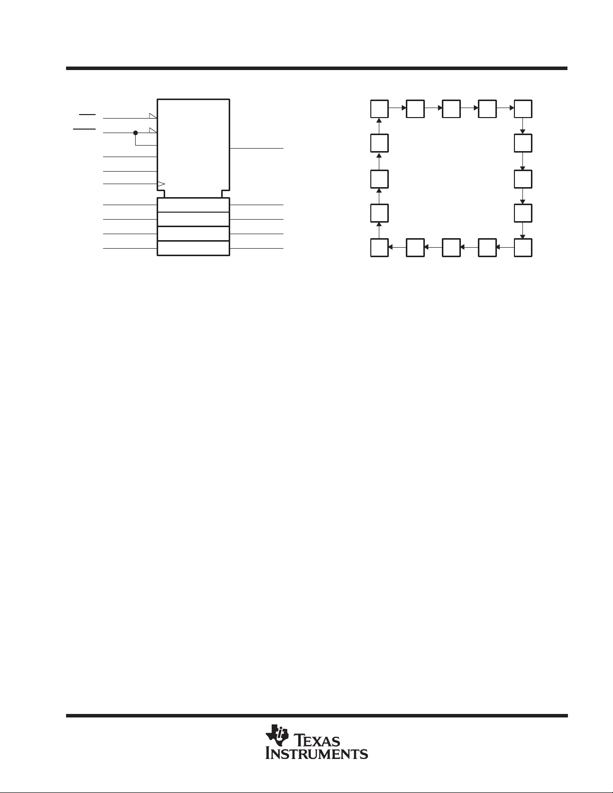
†
CTRDIV16
CT = 0
M1
M2
G3
G4
1, 5D
3CT = 15
C5/2,3,4+
1
2
4
8
logic symbol
CLR
LOAD
ENT
ENP
CLK
A
B
C
D
†
This symbol is in accordance with ANSI/IEEE Std 91-1984 and
IEC Publication 617-12.
15
14
13
12
11
state diagram
RCO
Q
A
Q
B
Q
C
Q
D
15
14
13
12
0
1234
5
6
7
891011
2–2
POST OFFICE BOX 655303 • DALLAS, TEXAS 75265
logic diagram (positive logic)
SN74F161A
SYNCHRONOUS 4-BIT BINARY COUNTER
SDFS056A – D2932, MARCH 1987 – REVISED OCT OBER 1993
CLR
LOAD
ENT
ENP
CLK
1
9
10
7
R
2
3
A
4
B
G2
1
1, 3D
M1
R
G2
1
1, 3D
M1
, 2T/C3
, 2T/C3
15
14
13
RCO
Q
A
Q
B
R
G2
, 2T/C3
5
C
6
D
1
1, 3D
M1
R
G2
1
1, 3D
M1
, 2T/C3
12
11
Q
C
Q
D
POST OFFICE BOX 655303 • DALLAS, TEXAS 75265
2–3

SN74F161A
SYNCHRONOUS 4-BIT BINARY COUNTER
SDFS056A – D2932, MARCH 1987 – REVISED OCT OBER 1993
logic symbol, each flip-flop
R
CLK
R
G2TE
1, 3DD
M1LOAD
logic diagram, each flip-flop (positive logic)
R
TE
(Toggle
Enable)
CLK
D
1, 2T/C3
Q1
Q1
Q2
Q
2
Q1
Q2
LOAD
2–4
POST OFFICE BOX 655303 • DALLAS, TEXAS 75265
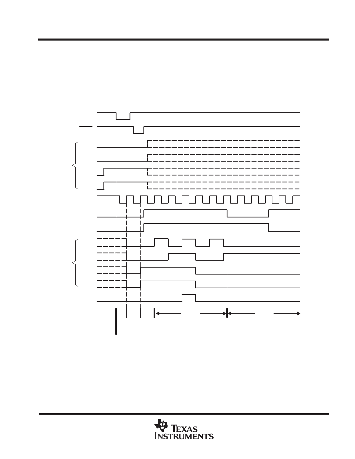
typical clear, preset, count, and inhibit sequences
Illustrated below is the following sequence:
1. Clear outputs to zero
2. Preset to binary twelve
3. Count to thirteen, fourteen, fifteen, zero, one, and two
4. Inhibit
CLR
LOAD
A
SN74F161A
SYNCHRONOUS 4-BIT BINARY COUNTER
SDFS056A – D2932, MARCH 1987 – REVISED OCT OBER 1993
Data
Inputs
Data
Outputs
CLK
ENP
ENT
Q
Q
Q
Q
RCO
B
C
D
A
B
C
D
14 15 0 1 2
Count Inhibit
Sync
Clear
12 13
Preset
Async
Clear
POST OFFICE BOX 655303 • DALLAS, TEXAS 75265
2–5

SN74F161A
V
V
SYNCHRONOUS 4-BIT BINARY COUNTER
SDFS056A – D2932, MARCH 1987 – REVISED OCT OBER 1993
absolute maximum ratings over operating free-air temperature range (unless otherwise noted)
Supply voltage range, V
Input voltage range, V
Input current range –30 mA to 5 mA. . . . . . . . . . . . . . . . . . . . . . . . . . . . . . . . . . . . . . . . . . . . . . . . . . . . . . . . . . . . . .
Voltage range applied to any output in the high state –0.5 V to V
Current into any output in the low state 40 mA. . . . . . . . . . . . . . . . . . . . . . . . . . . . . . . . . . . . . . . . . . . . . . . . . . . . .
Operating free-air temperature range 0°C to 70°C. . . . . . . . . . . . . . . . . . . . . . . . . . . . . . . . . . . . . . . . . . . . . . . . . .
Storage temperature range –65°C to 150°C. . . . . . . . . . . . . . . . . . . . . . . . . . . . . . . . . . . . . . . . . . . . . . . . . . . . . . .
†
Stresses beyond those listed under “absolute maximum ratings” may cause permanent damage to the device. These are stress ratings only and
functional operation of the device at these or any other conditions beyond those indicated under “recommended operating conditions” is not
implied. Exposure to absolute-maximum-rated conditions for extended periods may affect device reliability.
NOTE 1: The input voltage ratings may be exceeded provided the input current ratings are observed.
–0.5 V to 7 V. . . . . . . . . . . . . . . . . . . . . . . . . . . . . . . . . . . . . . . . . . . . . . . . . . . . . . . . . .
CC
(see Note 1) –1.2 V to 7 V. . . . . . . . . . . . . . . . . . . . . . . . . . . . . . . . . . . . . . . . . . . . . . . . . .
I
. . . . . . . . . . . . . . . . . . . . . . . . . . . . . . . . . .
recommended operating conditions
MIN NOM MAX UNIT
V
V
V
I
I
I
T
CC
IH
IL
IK
OH
OL
A
Supply voltage 4.5 5 5.5 V
High-level input voltage 2 V
Low-level input voltage 0.8 V
Input clamp current –18 mA
High-level output current –1 mA
Low-level output current 20 mA
Operating free-air temperature 0 70 °C
†
CC
electrical characteristics over recommended operating free-air temperature range (unless
otherwise noted)
PARAMETER TEST CONDITIONS MIN TYP‡MAX UNIT
V
IK
OH
V
OL
I
I
I
IH
ENP, CLK, A, B, C, D – 0.6
I
ENT, LOAD
IL
CLR – 0.6
§
I
OS
I
CC
‡
All typical values are at VCC = 5 V, TA = 25°C.
§
Not more than one output should be shorted at a time, and the duration of the short circuit should not exceed one second.
VCC = 4.5 V, II = –18 mA –1.2 V
VCC = 4.5 V, IOH = – 1 mA 2.5 3.4
VCC = 4.75 V, IOH = – 1 mA 2.7
VCC = 4.5 V, IOL = 20 mA 0.3 0.5 V
VCC = 5.5 V, VI = 7 V 0.1 mA
VCC = 5.5 V, VI = 2.7 V 20 µA
VCC = 5.5 V, VI = 0.5 V
VCC = 5.5 V, VO = 0 –60 –150 mA
VCC = 5.5 V 37 55 mA
– 1.2
mA
2–6
POST OFFICE BOX 655303 • DALLAS, TEXAS 75265

SN74F161A
twPulse duration
CLK (counting)
ns
LOAD bef
CLK↑
ENP and ENT before CLK↑
thHold time
LOAD aft
CLK↑
ns
CLK (LOAD high)
A
Q
ns
CLK (LOAD low)
A
Q
ns
CLK
RCO
ns
ENT
RCO
ns
t
CLR
ns
SYNCHRONOUS 4-BIT BINARY COUNTER
SDFS056A – D2932, MARCH 1987 – REVISED OCT OBER 1993
timing requirements over recommended ranges of supply voltage and operating free-air
temperature (unless otherwise noted)
VCC = 5 V,
f
clock
t
su
t
su
†
Inactive-state state setup time is also referred to as recovery time.
Clock frequency 0 100 0 90 MHz
CLK high or low (loading) 5 5
CLR low 5 5
Data before CLK↑ High or low 5 5
Setup time
Data after CLK↑ High or low 2 2
ENP and ENT after CLK↑ High or low 0 0
Inactive-state setup time, CLR high before CLK↑
ore
er
†
TA = 25°C
MIN MAX
High 4 4
Low 6 7
High 11 11.5
Low 8.5 9.5
High 11 11.5
Low 5 5
High 2 2
Low 0 0
6 6 ns
MIN MAX UNIT
ns
switching characteristics (see Note 2)
VCC = 5 V,
PARAMETER
f
max
t
PLH
t
PHL
t
PLH
t
PHL
t
PLH
t
PHL
t
PLH
t
PHL
PHL
‡
For conditions shown as MIN or MAX, use the appropriate value specified under recommended operating conditions.
NOTE 2: Load circuits and waveforms are shown in Section 1.
FROM
(INPUT)
TO
(OUTPUT)
ny
ny
Any Q
RCO
CL = 50 pF,
RL = 500 Ω,
TA = 25°C
MIN TYP MAX MIN MAX
100 120 90 MHz
2.7 5.1 7.5 2.7 8.5
2.7 7.1 10 2.7 11
3.2 5.6 8.5 3.2 9.5
3.2 5.6 8.5 3.2 9.5
4.2 9.6 14 4.2 15
4.2 9.6 14 4.2 15
1.7 4.1 7.5 1.7 8.5
1.7 4.1 7.5 1.7 8.5
4.7 8.6 12 4.7 13
3.7 7.6 10.5 3.7 11.5
VCC = 4.5 V to 5.5 V,
CL = 50 pF,
RL = 500Ω,
TA = MIN to MAX
UNIT
‡
POST OFFICE BOX 655303 • DALLAS, TEXAS 75265
2–7

SN74F161A
SYNCHRONOUS 4-BIT BINARY COUNTER
SDFS056A – D2932, MARCH 1987 – REVISED OCT OBER 1993
2–8
POST OFFICE BOX 655303 • DALLAS, TEXAS 75265

IMPORTANT NOTICE
T exas Instruments and its subsidiaries (TI) reserve the right to make changes to their products or to discontinue
any product or service without notice, and advise customers to obtain the latest version of relevant information
to verify, before placing orders, that information being relied on is current and complete. All products are sold
subject to the terms and conditions of sale supplied at the time of order acknowledgement, including those
pertaining to warranty, patent infringement, and limitation of liability.
TI warrants performance of its semiconductor products to the specifications applicable at the time of sale in
accordance with TI’s standard warranty. Testing and other quality control techniques are utilized to the extent
TI deems necessary to support this warranty . Specific testing of all parameters of each device is not necessarily
performed, except those mandated by government requirements.
CERT AIN APPLICATIONS USING SEMICONDUCTOR PRODUCTS MAY INVOLVE POTENTIAL RISKS OF
DEATH, PERSONAL INJURY, OR SEVERE PROPERTY OR ENVIRONMENTAL DAMAGE (“CRITICAL
APPLICATIONS”). TI SEMICONDUCTOR PRODUCTS ARE NOT DESIGNED, AUTHORIZED, OR
WARRANTED TO BE SUITABLE FOR USE IN LIFE-SUPPORT DEVICES OR SYSTEMS OR OTHER
CRITICAL APPLICA TIONS. INCLUSION OF TI PRODUCTS IN SUCH APPLICATIONS IS UNDERST OOD TO
BE FULLY AT THE CUSTOMER’S RISK.
In order to minimize risks associated with the customer’s applications, adequate design and operating
safeguards must be provided by the customer to minimize inherent or procedural hazards.
TI assumes no liability for applications assistance or customer product design. TI does not warrant or represent
that any license, either express or implied, is granted under any patent right, copyright, mask work right, or other
intellectual property right of TI covering or relating to any combination, machine, or process in which such
semiconductor products or services might be or are used. TI’s publication of information regarding any third
party’s products or services does not constitute TI’s approval, warranty or endorsement thereof.
Copyright 1998, Texas Instruments Incorporated
 Loading...