

SN74F112
DUAL NEGATIVE-EDGE-TRIGGERED J-K FLIP-FLOP
WITH CLEAR AND PRESET
SDFS048A – D2932, MARCH 1987 – REVISED OCTOBER 1993
Copyright 1993, Texas Instruments Incorporated
2–1
POST OFFICE BOX 655303 • DALLAS, TEXAS 75265
• Package Options Include Plastic
Small-Outline Packages and Standard
Plastic 300-mil DIPs
description
The SN74F112 contains two independent J-K
negative-edge-triggered flip-flops. A low level at
the preset (PRE
) or clear (CLR) inputs sets or
resets the outputs regardless of the levels of the
other inputs. When PRE
and CLR are inactive
(high), data at the J and K inputs meeting the setup
time requirements is transferred to the outputs on
the negative-going edge of the clock pulse. Clock
triggering occurs at a voltage level and is not
directly related to the rise time of the clock pulse.
Following the hold-time interval, data at the J and
K inputs may be changed without affecting the
levels at the outputs. The SN74F1 12 can perform
as a toggle flip-flop by tying J and K high.
The SN74F1 12 is characterized for operation from
0°C to 70°C.
FUNCTION TABLE
INPUTS
OUTPUTS
PRE CLR CLK J K Q Q
L H X X X H L
H LXXXLH
LLXXXH
†
H
†
HH↓LLQ
0
Q
0
HH↓HLHL
HH↓LHLH
HH↓H H Toggle
H H H X X Q
0
Q
0
†
The output levels in this configuration are not guaranteed to
meet the minimum levels for VOH. Furthermore, this
configuration is nonstable; that is, it will not persist when
either PRE
or CLR returns to its inactive (high) level.
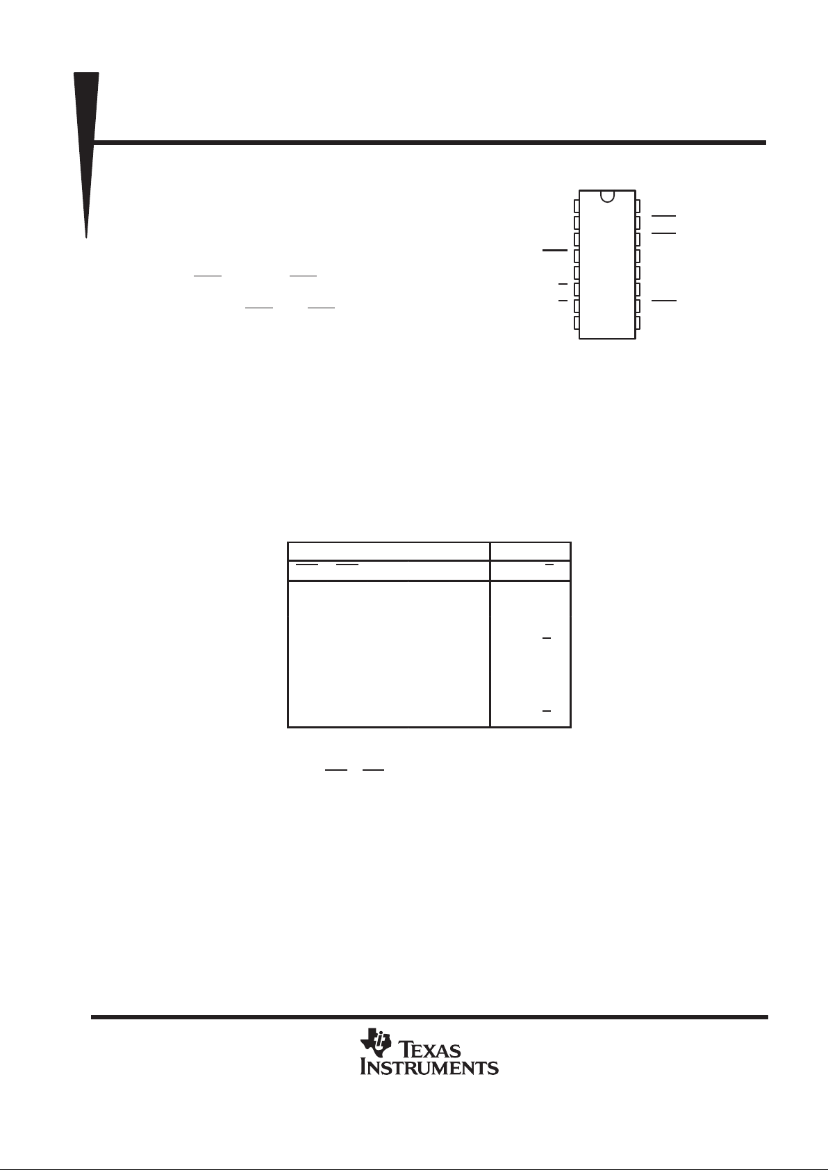
D OR N PACKAGE
(TOP VIEW)
1
2
3
4
5
6
7
8
16
15
14
13
12
11
10
9
1CLK
1K
1J
1PRE
1Q
1Q
2Q
GND
V
CC
1CLR
2CLR
2CLK
2K
2J
2PRE
2Q
PRODUCTION DATA information is current as of publication date.
Products conform to specifications per the terms of Texas Instruments
standard warranty. Production processing does not necessarily include
testing of all parameters.
SN74F112
DUAL NEGATIVE-EDGE-TRIGGERED J-K FLIP-FLOP
WITH CLEAR AND PRESET
SDFS048A – D2932, MARCH 1987 – REVISED OCT OBER 1993
2–2
POST OFFICE BOX 655303 • DALLAS, TEXAS 75265
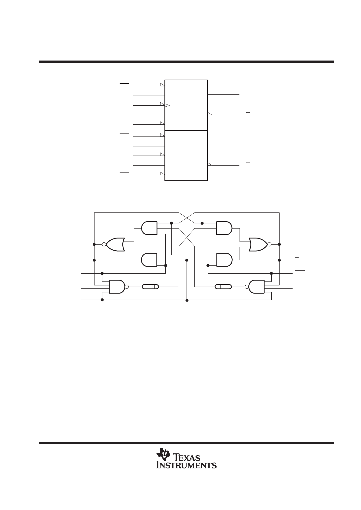
logic symbol
†
S
4
1J
3
1J
1K
2
1K
R
15
1Q
5
6
C1
1PRE
1CLR
1Q
1
1CLK
10
11
2J
12
2K
14
2Q
9
7
2PRE
2CLR
2Q
13
2CLK
†
This symbol is in accordance with ANSI/IEEE Std 91-1984 and IEC Publication 617-12.
logic diagram, each flip-flop (positive logic)
PRE
CLK
K
Q Q
CLR
J
absolute maximum ratings over operating free-air temperature range (unless otherwise noted)
‡
Supply voltage range, V
CC
–0.5 V to 7 V. . . . . . . . . . . . . . . . . . . . . . . . . . . . . . . . . . . . . . . . . . . . . . . . . . . . . . . . . .
Input voltage range, V
I
(see Note 1) –1.2 V to 7 V. . . . . . . . . . . . . . . . . . . . . . . . . . . . . . . . . . . . . . . . . . . . . . . . . .
Input current range –30 mA to 5 mA. . . . . . . . . . . . . . . . . . . . . . . . . . . . . . . . . . . . . . . . . . . . . . . . . . . . . . . . . . . . . .
Voltage range applied to any output in the high state –0.5 V to V
CC
. . . . . . . . . . . . . . . . . . . . . . . . . . . . . . . . . .
Current into any output in the low state 40 mA. . . . . . . . . . . . . . . . . . . . . . . . . . . . . . . . . . . . . . . . . . . . . . . . . . . . .
Operating free-air temperature range 0°C to 70°C. . . . . . . . . . . . . . . . . . . . . . . . . . . . . . . . . . . . . . . . . . . . . . . . . .
Storage temperature range –65°C to 150°C. . . . . . . . . . . . . . . . . . . . . . . . . . . . . . . . . . . . . . . . . . . . . . . . . . . . . . .
‡
Stresses beyond those listed under “absolute maximum ratings” may cause permanent damage to the device. These are stress ratings only and
functional operation of the device at these or any other conditions beyond those indicated under “recommended operating conditions” is not
implied. Exposure to absolute-maximum-rated conditions for extended periods may affect device reliability.
NOTE 1: The input voltage ratings may be exceeded provided the input current ratings are observed.
SN74F112
DUAL NEGATIVE-EDGE-TRIGGERED J-K FLIP-FLOP
WITH CLEAR AND PRESET
SDFS048A – D2932, MARCH 1987 – REVISED OCTOBER 1993
2–3
POST OFFICE BOX 655303 • DALLAS, TEXAS 75265
recommended operating conditions
MIN NOM MAX UNIT
V
CC
Supply voltage 4.5 5 5.5 V
V
IH
High-level input voltage 2 V
V
IL
Low-level input voltage 0.8 V
I
IK
Input clamp current –18 mA
I
OH
High-level output current –1 mA
I
OL
Low-level output current 20 mA
T
A
Operating free-air temperature 0 70 °C
electrical characteristics over recommended operating free-air temperature range (unless
otherwise noted)
PARAMETER TEST CONDITIONS MIN TYP†MAX UNIT
V
IK
VCC = 4.5 V, II = –18 mA –1.2 V
VCC = 4.5 V, IOH = – 1 mA 2.5 3.4
V
OH
VCC = 4.75 V , IOH = – 1 mA 2.7
V
V
OL
VCC = 4.5 V, IOL = 20 mA 0.3 0.5 V
I
I
VCC = 5.5 V, VI = 7 V 0.1 mA
I
IH
VCC = 5.5 V, VI = 2.7 V 20 µA
J or K – 0.6
I
IL
PRE or CLR
VCC = 5.5 V, VI = 0.5 V
–3
mA
CLK – 2.4
I
OS
‡
VCC = 5.5 V, VO = 0 –60 –150 mA
I
CC
VCC = 5.5 V, See Note 2 12 19 mA
†
All typical values are at VCC = 5 V, TA = 25°C.
‡
Not more than one output should be shorted at a time, and the duration of the short circuit should not exceed one second.
NOTE 2: ICC is measured with all outputs open, the Q and Q
outputs alternately high and the clock input grounded at the time of measurement.
timing requirements over recommended ranges of supply voltage and operating free-air
temperature (unless otherwise noted)
VCC = 5 V,
TA = 25°C
MIN MAX UNIT
MIN MAX
f
clock
Clock frequency 0 110 0 100 MHz
CLK high or low 4.5 5
twPulse duration
CLR or PRE low 4.5 5
ns
p
High 4 5
tsuSetup time, data before CLK↓
Low 3 3.5
ns
High 0 0
thHold time, data after CLK↓
Low 0 0
ns
t
su
Setup time, inactive state, data before CLK↓
§
CLR or PRE high 4 5 ns
§
Inactive-state state setup time is also referred to as recovery time.
SN74F112
DUAL NEGATIVE-EDGE-TRIGGERED J-K FLIP-FLOP
WITH CLEAR AND PRESET
SDFS048A – D2932, MARCH 1987 – REVISED OCT OBER 1993
2–4
POST OFFICE BOX 655303 • DALLAS, TEXAS 75265
switching characteristics (see Note 3)
PARAMETER
FROM
(INPUT)
TO
(OUTPUT)
VCC = 5 V,
CL = 50 pF,
RL = 500 Ω,
TA = 25°C
VCC = 4.5 V to 5.5 V,
CL = 50 pF,
RL = 500Ω,
TA = MIN to MAX
†
UNIT
MIN TYP MAX MIN MAX
f
max
110 130 100 MHz
t
PLH
1.2 4.6 6.5 1.2 7.5
t
PHL
CLK
Q
or
Q
1.2 4.6 6.5 1.2 7.5
ns
t
PLH
1.2 4.1 6.5 1.2 7.5
t
PHL
PRE or CLR
Q or Q
1.2 4.1 6.5 1.2 7.5
ns
†
For conditions shown as MIN or MAX, use the appropriate value specified under recommended operating conditions.
NOTE 3: Load circuits and waveforms are shown in Section 1.

IMPORTANT NOTICE
T exas Instruments and its subsidiaries (TI) reserve the right to make changes to their products or to discontinue
any product or service without notice, and advise customers to obtain the latest version of relevant information
to verify, before placing orders, that information being relied on is current and complete. All products are sold
subject to the terms and conditions of sale supplied at the time of order acknowledgement, including those
pertaining to warranty, patent infringement, and limitation of liability.
TI warrants performance of its semiconductor products to the specifications applicable at the time of sale in
accordance with TI’s standard warranty. Testing and other quality control techniques are utilized to the extent
TI deems necessary to support this warranty. Specific testing of all parameters of each device is not necessarily
performed, except those mandated by government requirements.
CERT AIN APPLICATIONS USING SEMICONDUCTOR PRODUCTS MAY INVOLVE POTENTIAL RISKS OF
DEATH, PERSONAL INJURY, OR SEVERE PROPERTY OR ENVIRONMENTAL DAMAGE (“CRITICAL
APPLICATIONS”). TI SEMICONDUCTOR PRODUCTS ARE NOT DESIGNED, AUTHORIZED, OR
WARRANTED TO BE SUITABLE FOR USE IN LIFE-SUPPORT DEVICES OR SYSTEMS OR OTHER
CRITICAL APPLICATIONS. INCLUSION OF TI PRODUCTS IN SUCH APPLICA TIONS IS UNDERST OOD TO
BE FULLY AT THE CUSTOMER’S RISK.
In order to minimize risks associated with the customer’s applications, adequate design and operating
safeguards must be provided by the customer to minimize inherent or procedural hazards.
TI assumes no liability for applications assistance or customer product design. TI does not warrant or represent
that any license, either express or implied, is granted under any patent right, copyright, mask work right, or other
intellectual property right of TI covering or relating to any combination, machine, or process in which such
semiconductor products or services might be or are used. TI’s publication of information regarding any third
party’s products or services does not constitute TI’s approval, warranty or endorsement thereof.
Copyright 1998, Texas Instruments Incorporated
 Loading...