

Texas Instruments SN74CBTLV3126D, SN74CBTLV3126DBQR, SN74CBTLV3126DGVR, SN74CBTLV3126DR, SN74CBTLV3126PWR Datasheet
SN74CBTLV3126
LOW-VOLTAGE QUADRUPLE FET BUS SWITCH
SCDS038D – DECEMBER 1997 – REVISED JUL Y 1999
D
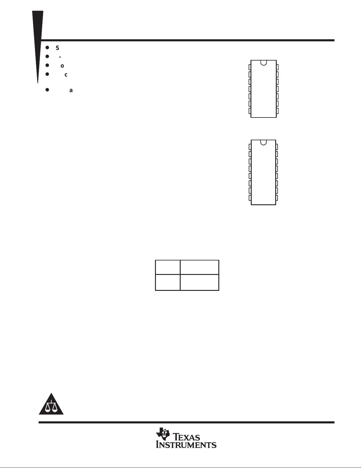
Standard ’126-Type Pinout
D
5-Ω Switch Connection Between Two Ports
D
Isolation Under Power-Off Conditions
D
Latch-up Performance Exceeds 100 mA per
JESD 78, Class II
D
Package Options Include Plastic
Small-Outline (D), Shrink Small-Outline
(DBQ), Thin Very Small-Outline (DGV), and
Thin Shrink Small-Outline (PW) Packages
description
The SN74CBTL V3126 quadruple FET bus switch
features independent line switches. Each switch
is disabled when the associated output-enable
(OE) input is low.
T o ensure the high-impedance state during power
up or power down, OE should be tied to GND
through a pulldown resistor; the minimum value of
the resistor is determined by the current-sinking
capability of the driver.
The SN74CBTLV3126 is characterized for
operation from –40°C to 85°C.
D, DGV, OR PW PACKAGE
(TOP VIEW)
16
15
14
13
12
11
10
14
13
12
11
10
V
CC
4OE
4A
4B
3OE
9
3A
8
3B
V
CC
4OE
4A
4B
3OE
3A
3B
9
NC
1OE
1
1A
2
1B
3
4
2OE
5
2A
6
2B
7
GND
DBQ PACKAGE
(TOP VIEW)
1
NC
2
1OE
3
1A
4
1B
5
2OE
6
2A
7
2B
8
GND
NC – No internal connection
FUNCTION TABLE
(each bus switch)
INPUT
OE
L Disconnect
H A port = B port
Please be aware that an important notice concerning availability, standard warranty, and use in critical applications of
Texas Instruments semiconductor products and disclaimers thereto appears at the end of this data sheet.
FUNCTION
PRODUCTION DATA information is current as of publication date.
Products conform to specifications per the terms of Texas Instruments
standard warranty. Production processing does not necessarily include
testing of all parameters.
POST OFFICE BOX 655303 • DALLAS, TEXAS 75265
Copyright 1999, Texas Instruments Incorporated
1
SN74CBTLV3126
LOW-VOLTAGE QUADRUPLE FET BUS SWITCH
SCDS038D – DECEMBER 1997 – REVISED JUL Y 1999
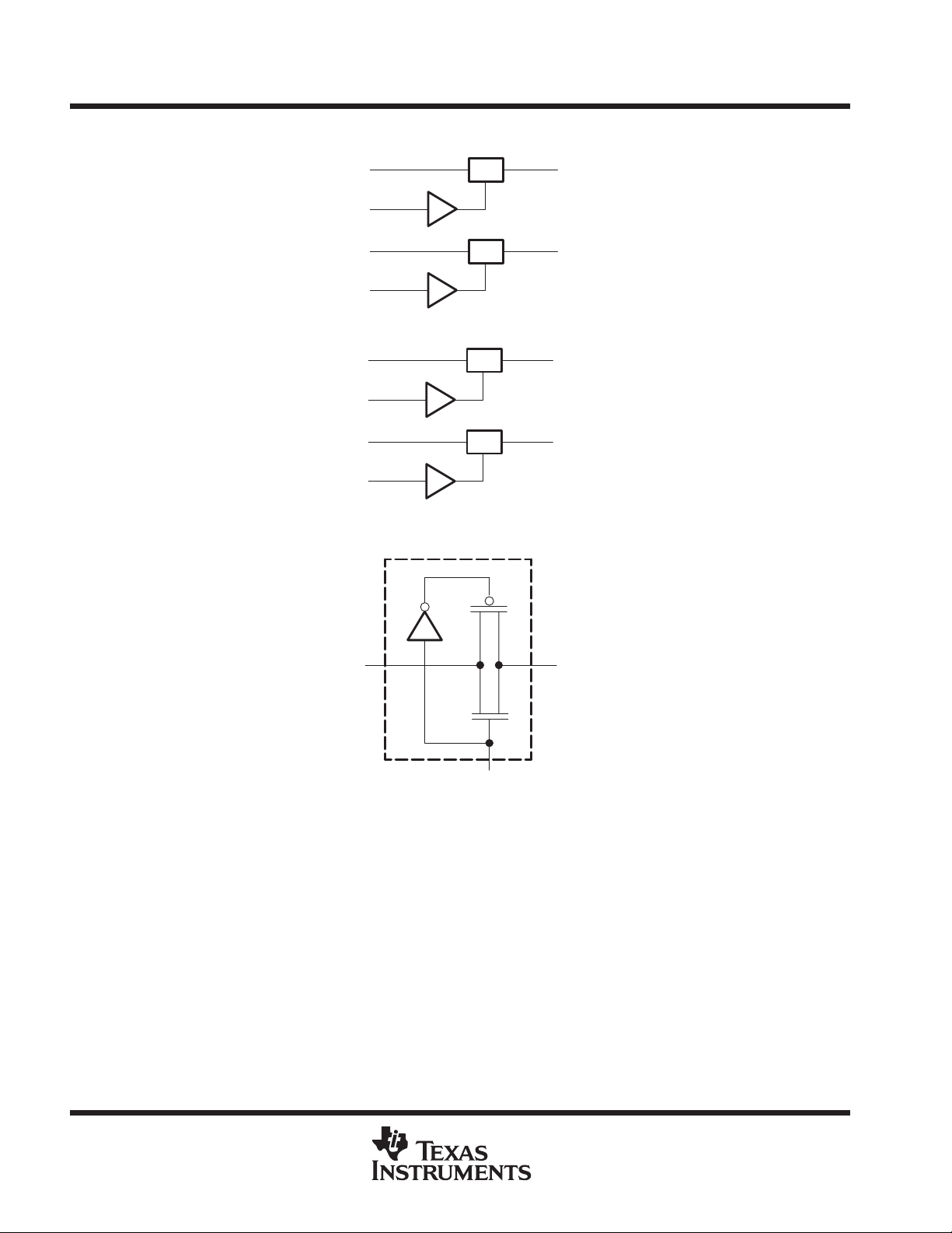
logic diagram (positive logic)
1A
1OE
2A
2OE
3A
3OE
4A
4OE
simplified schematic, each FET switch
2
1
5
4
9
10
12
13
SW
SW
SW
SW
3
1B
6
2B
8
3B
11
4B
A
(OE)
B
absolute maximum ratings over operating free-air temperature range (unless otherwise noted)
Supply voltage range, VCC –0.5 V to 4.6 V. . . . . . . . . . . . . . . . . . . . . . . . . . . . . . . . . . . . . . . . . . . . . . . . . . . . . . . . .
Input voltage range, VI (see Note 1) –0.5 V to 4.6 V. . . . . . . . . . . . . . . . . . . . . . . . . . . . . . . . . . . . . . . . . . . . . . . . .
Continuous channel current 128 mA. . . . . . . . . . . . . . . . . . . . . . . . . . . . . . . . . . . . . . . . . . . . . . . . . . . . . . . . . . . . . .
Input clamp current, I
Package thermal impedance, θ
Storage temperature range, T
†
Stresses beyond those listed under “absolute maximum ratings” may cause permanent damage to the device. These are stress ratings only, and
functional operation of the device at these or any other conditions beyond those indicated under “recommended operating conditions” is not
implied. Exposure to absolute-maximum-rated conditions for extended periods may affect device reliability.
NOTES: 1. The input and output negative-voltage ratings may be exceeded if the input and output clamp-current ratings are observed.
2. The package thermal impedance is calculated in accordance with JESD 51.
IK
(V
< 0) –50 mA. . . . . . . . . . . . . . . . . . . . . . . . . . . . . . . . . . . . . . . . . . . . . . . . . . . . . . . . .
I/O
(see Note 2): D package 127°C/W. . . . . . . . . . . . . . . . . . . . . . . . . . . . . . . . . .
JA
DBQ package 139°C/W. . . . . . . . . . . . . . . . . . . . . . . . . . . . . . .
DGV package 182°C/W. . . . . . . . . . . . . . . . . . . . . . . . . . . . . . .
PW package 170°C/W. . . . . . . . . . . . . . . . . . . . . . . . . . . . . . . .
–65°C to 150°C. . . . . . . . . . . . . . . . . . . . . . . . . . . . . . . . . . . . . . . . . . . . . . . . . . .
stg
†
2
POST OFFICE BOX 655303 • DALLAS, TEXAS 75265
 Loading...