

Texas Instruments SN74CBTLV3125D, SN74CBTLV3125DBQR, SN74CBTLV3125DGVR, SN74CBTLV3125DR, SN74CBTLV3125PWR Datasheet
SN74CBTLV3125
LOW-VOLTAGE QUADRUPLE FET BUS SWITCH
SCDS037D – DECEMBER 1997 – REVISED JUL Y 1999
D
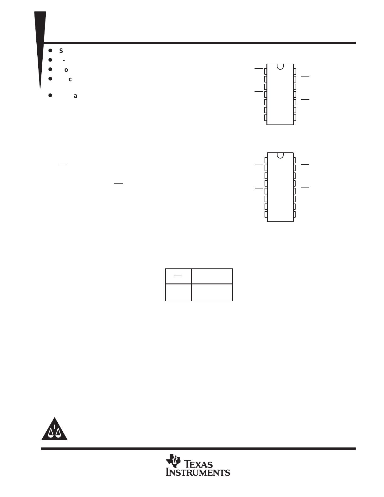
Standard ’125-Type Pinout
D
5-Ω Switch Connection Between Two Ports
D
Isolation Under Power-Off Conditions
D
Latch-Up Performance Exceeds 100 mA Per
JESD 78, Class II
D
Package Options Include Plastic
Small-Outline (D), Shrink Small-Outline
(DBQ), Thin Very Small-Outline (DGV), and
Thin Shrink Small-Outline (PW) Packages
description
The SN74CBTL V3125 quadruple FET bus switch
features independent line switches. Each switch
is disabled when the associated output-enable
(OE
) input is high.
T o ensure the high-impedance state during power
up or power down, OE should be tied to V
through a pullup resistor; the minimum value of
the resistor is determined by the current-sinking
capability of the driver.
The SN74CBTLV3125 is characterized for
operation from –40°C to 85°C.
CC
D, DGV, OR PW PACKAGE
(TOP VIEW)
16
15
14
13
12
11
10
14
13
12
11
10
V
CC
4OE
4A
4B
3OE
9
3A
8
3B
V
CC
4OE
4A
4B
3OE
3A
3B
9
NC
1OE
1
1A
2
1B
3
4
2OE
5
2A
6
2B
GND
GND
NC – No internal connection
7
DBQ PACKAGE
(TOP VIEW)
1
NC
2
1OE
3
1A
4
1B
5
2OE
6
2A
7
2B
8
FUNCTION TABLE
(each bus switch)
INPUT
OE
L A port = B port
H Disconnect
Please be aware that an important notice concerning availability, standard warranty, and use in critical applications of
Texas Instruments semiconductor products and disclaimers thereto appears at the end of this data sheet.
FUNCTION
PRODUCTION DATA information is current as of publication date.
Products conform to specifications per the terms of Texas Instruments
standard warranty. Production processing does not necessarily include
testing of all parameters.
POST OFFICE BOX 655303 • DALLAS, TEXAS 75265
Copyright 1999, Texas Instruments Incorporated
1
SN74CBTLV3125
LOW-VOLTAGE QUADRUPLE FET BUS SWITCH
SCDS037D – DECEMBER 1997 – REVISED JUL Y 1999
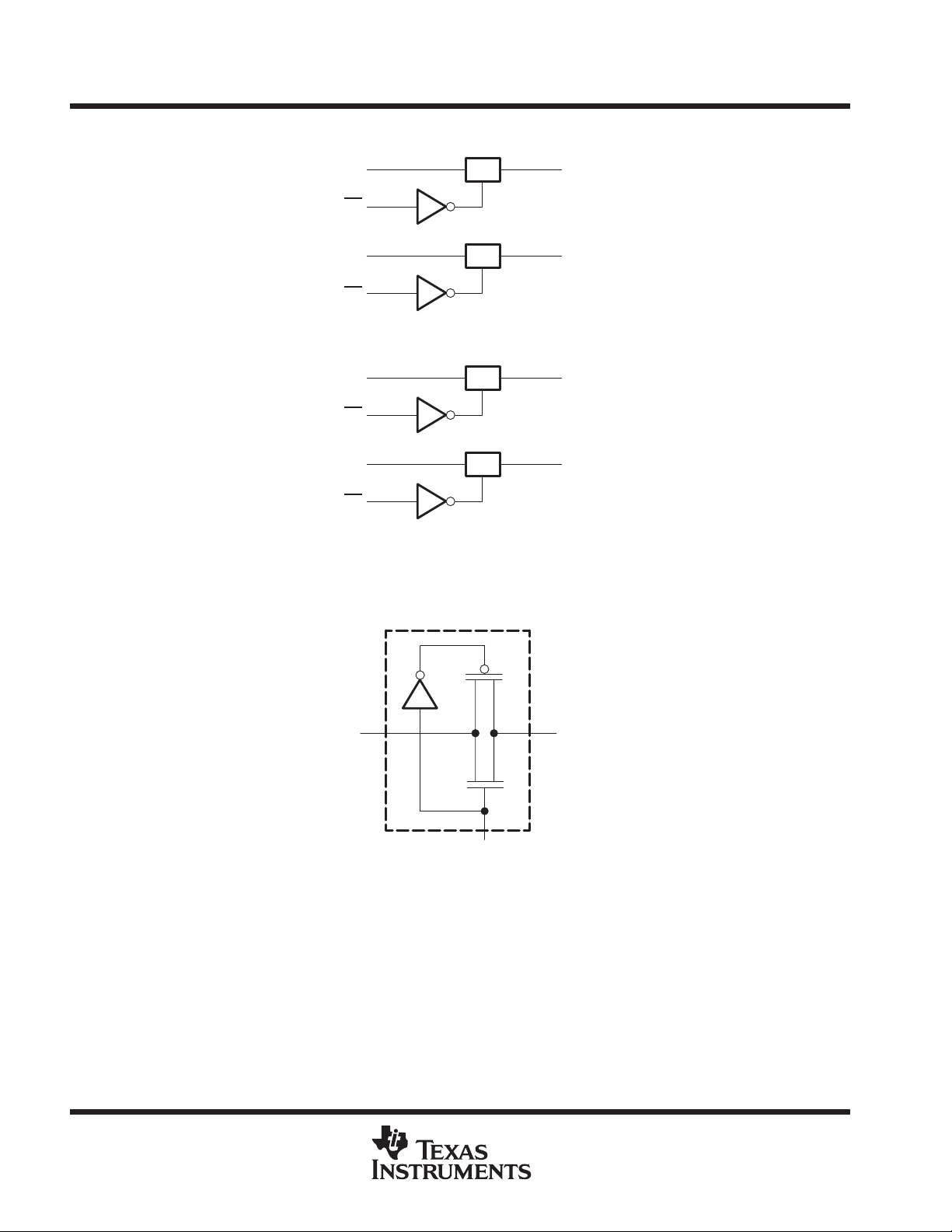
logic diagram (positive logic)
2
1A
1
1OE
5
2A
4
2OE
9
3A
10
3OE
12
4A
13
4OE
Pin numbers shown are for the D, DGV, and PW packages.
simplified schematic, each FET switch
SW
SW
SW
SW
3
1B
6
2B
8
3B
11
4B
A
(OE)
B
2
POST OFFICE BOX 655303 • DALLAS, TEXAS 75265
 Loading...