

Texas Instruments SN74CBTLV16292DL, SN74CBTLV16292DLR, SN74CBTLV16292GR, SN74CBTLV16292VR Datasheet
SN74CBTLV16292
LOW-VOLTAGE 12-BIT 1-OF-2 FET MULTIPLEXER/DEMULTIPLEXER
WITH INTERNAL PULLDOWN RESISTORS
SCDS055G – MARCH 1998 – REVISED APRIL 1999
D
4-Ω Switch Connection Between Two Ports
D
Isolation Under Power-Off Conditions
D
Make-Before-Break Feature
D
Internal 500-Ω Pulldown Resistors to
Ground
D
Latch-Up Performance Exceeds 250 mA Per
JESD 17
D
Package Options Include Plastic Thin
Shrink Small-Outline (DGG), Thin Very
Small-Outline (DGV), and 300-mil Shrink
Small-Outline (DL) Packages
description
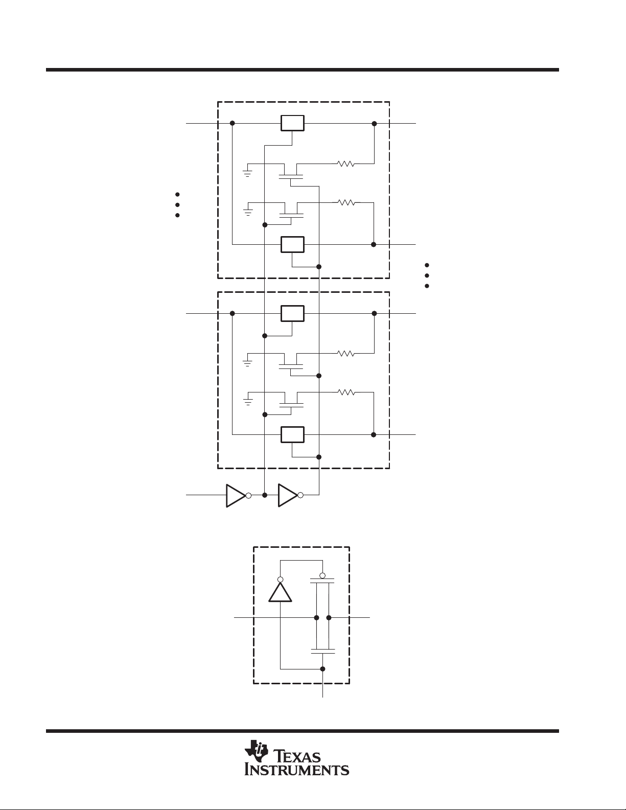
The SN74CBTLV16292 is a 12-bit 1-of-2
high-speed FET multiplexer/demultiplexer. The
low on-state resistance of the switch allows
connections to be made with minimal propagation
delay .
When the select (S) input is low, port A is
connected to port B1 and R
port B2. When S is high, port A is connected to
port B2 and R
is connected to port B1.
INT
The SN74CBTLV16292 is characterized for
operation from –40°C to 85°C.
FUNCTION TABLE
INPUT
S
L
H
FUNCTION
A port = B1 port
R
= B2 port
INT
A port = B2 port
R
= B1 port
INT
is connected to
INT
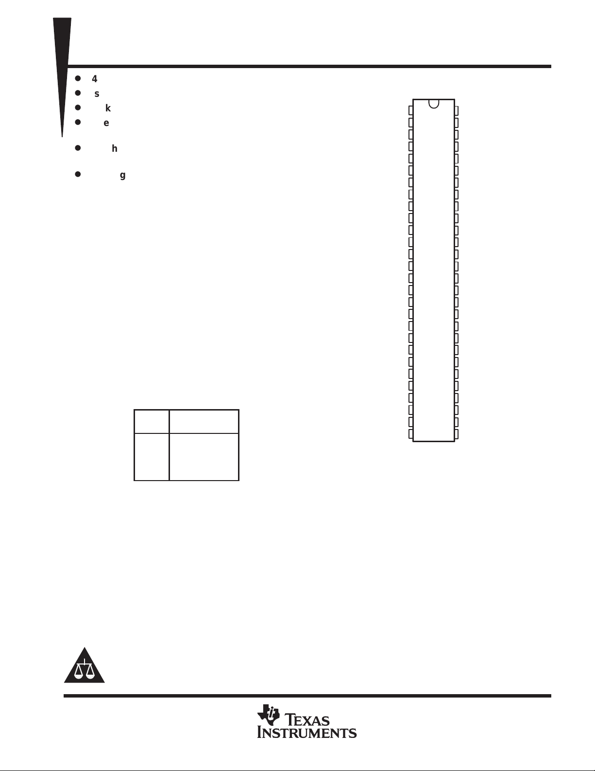
DGG, DGV, OR DL PACKAGE
(TOP VIEW)
1
2
3
4
5
6
7
8
9
10
11
12
13
14
15
16
17
18
19
20
21
22
23
24
25
26
27
28
56
55
54
53
52
51
50
49
48
47
46
45
44
43
42
41
40
39
38
37
36
35
34
33
32
31
30
29
NC
NC
1B1
1B2
2B1
2B2
3B1
GND
3B2
4B1
4B2
5B1
5B2
6B1
6B2
7B1
7B2
8B1
GND
8B2
9B1
9B2
10B1
10B2
1 1B1
1 1B2
12B1
12B2
S
1A
NC
2A
NC
3A
NC
GND
4A
NC
5A
NC
6A
NC
7A
NC
V
CC
8A
GND
NC
9A
NC
10A
NC
11A
NC
12A
NC
NC – No internal connection
Please be aware that an important notice concerning availability, standard warranty, and use in critical applications of
Texas Instruments semiconductor products and disclaimers thereto appears at the end of this data sheet.
PRODUCTION DATA information is current as of publication date.
Products conform to specifications per the terms of Texas Instruments
standard warranty. Production processing does not necessarily include
testing of all parameters.
POST OFFICE BOX 655303 • DALLAS, TEXAS 75265
Copyright 1999, Texas Instruments Incorporated
1
SN74CBTLV16292
LOW-VOLTAGE 12-BIT 1-OF-2 FET MULTIPLEXER/DEMULTIPLEXER
WITH INTERNAL PULLDOWN RESISTORS
SCDS055G – MARCH 1998 – REVISED APRIL 1999
logic diagram (positive logic)
1A
12A
2
27
SW
SW
SW
54
1B1
R
INT
R
INT
53
1B2
30
12B1
R
INT
R
INT
1
S
simplified schematic, each FET switch
A
SW
(OE)
29
12B2
B
2
POST OFFICE BOX 655303 • DALLAS, TEXAS 75265
VIHHigh-level control input voltage
V
VILLow-level control input voltage
V
V
V
0
TYP at V
CC
V
r
¶
Ω
V
0
SN74CBTLV16292
LOW-VOLTAGE 12-BIT 1-OF-2 FET MULTIPLEXER/DEMULTIPLEXER
WITH INTERNAL PULLDOWN RESISTORS
SCDS055G – MARCH 1998 – REVISED APRIL 1999
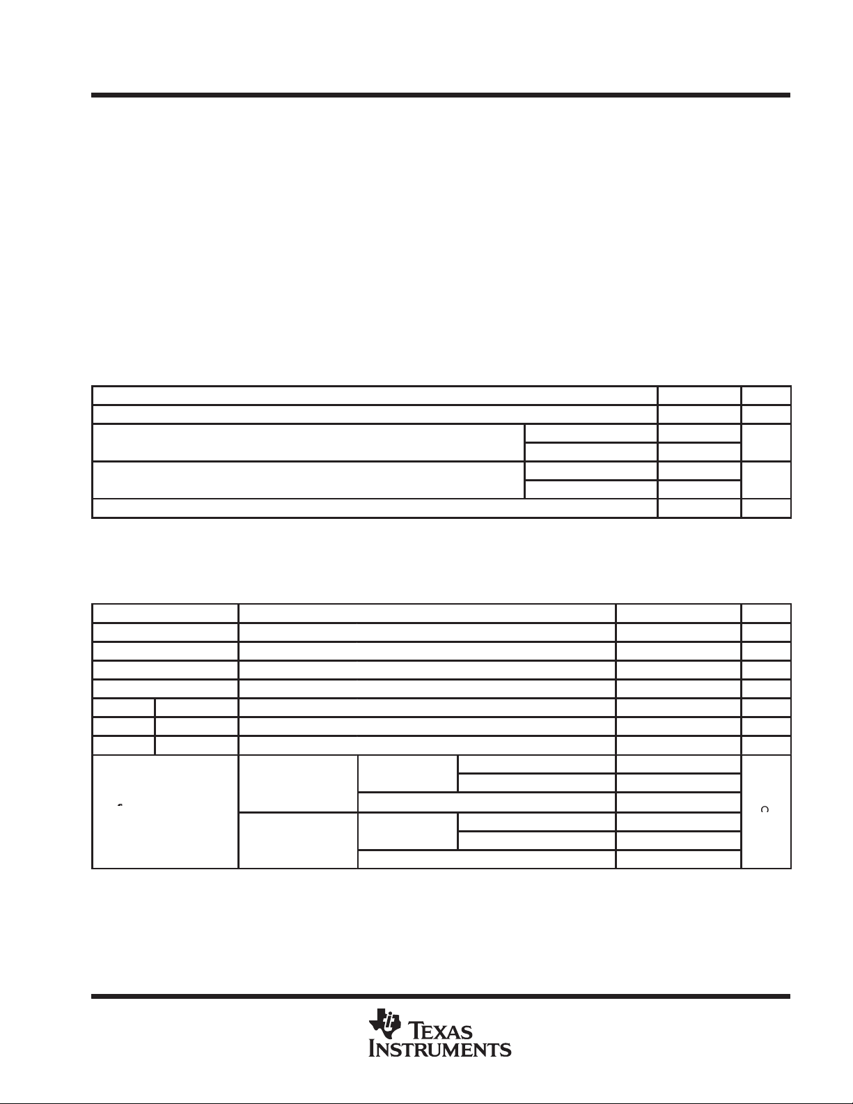
absolute maximum ratings over operating free-air temperature range (unless otherwise noted)
Supply voltage range, V
Input voltage range, V
–0.5 V to 4.6 V. . . . . . . . . . . . . . . . . . . . . . . . . . . . . . . . . . . . . . . . . . . . . . . . . . . . . . . . .
CC
(see Note 1) –0.5 V to 4.6 V. . . . . . . . . . . . . . . . . . . . . . . . . . . . . . . . . . . . . . . . . . . . . . . . .
I
†
Continuous channel current 128 mA. . . . . . . . . . . . . . . . . . . . . . . . . . . . . . . . . . . . . . . . . . . . . . . . . . . . . . . . . . . . . .
Input clamp current, I
Package thermal impedance, θ
(V
< 0) –50 mA. . . . . . . . . . . . . . . . . . . . . . . . . . . . . . . . . . . . . . . . . . . . . . . . . . . . . . . . . . .
IK
I
(see Note 2): DGG package 81°C/W. . . . . . . . . . . . . . . . . . . . . . . . . . . . . . . .
JA
DGV package 86°C/W. . . . . . . . . . . . . . . . . . . . . . . . . . . . . . . .
DL package 74°C/W. . . . . . . . . . . . . . . . . . . . . . . . . . . . . . . . . .
Storage temperature range, T
†
Stresses beyond those listed under “absolute maximum ratings” may cause permanent damage to the device. These are stress ratings only, and
functional operation of the device at these or any other conditions beyond those indicated under “recommended operating conditions” is not
implied. Exposure to absolute-maximum-rated conditions for extended periods may affect device reliability.
NOTES: 1. The input and output negative-voltage ratings may be exceeded if the input and output clamp-current ratings are observed.
2. The package thermal impedance is calculated in accordance with JESD 51.
–65°C to 150°C. . . . . . . . . . . . . . . . . . . . . . . . . . . . . . . . . . . . . . . . . . . . . . . . . . .
stg
recommended operating conditions (see Note 3)
MIN MAX UNIT
V
T
NOTE 3: All unused control inputs of the device must be held at VCC or GND to ensure proper device operation. Refer to the TI application report,
Supply voltage 2.3 3.6 V
CC
p
p
Operating free-air temperature –40 85 °C
A
Implications of Slow or Floating CMOS Inputs
, literature number SCBA004.
VCC = 2.3 V to 2.7 V 1.7
VCC = 2.7 V to 3.6 V 2
VCC = 2.3 V to 2.7 V 0.7
VCC = 2.7 V to 3.6 V 0.8
electrical characteristics over recommended operating free-air temperature range (unless
otherwise noted)
PARAMETER TEST CONDITIONS MIN TYP‡MAX UNIT
V
IK
I
I
I
off
I
CC
§
∆I
CC
C
i
C
io
on
‡
All typical values are at VCC = 3.3 V (unless otherwise noted), TA = 25°C.
§
This is the increase in supply current for each input that is at the specified voltage level rather than VCC or GND.
¶
Measured by the voltage drop between the A and B terminals at the indicated current through the switch. On-state resistance is determined by
the lower of the voltages of the two (A or B) terminals.
Control input VCC = 3.6 V, One input at 3 V, Other inputs at VCC or GND 300 µA
Control input VI = 3.3 V or 0 3.5 pF
A or B port VO = 3.3 V or 0 22.5 pF
VCC = 3 V, II = –18 mA –1.2 V
VCC = 3.6 V, VI = VCC or GND ±1 µA
VCC = 0, VI or VO = 0 to 3.6 V 10 µA
VCC = 3.6 V, IO = 0, VI = VCC or GND 10 µA
= 2.3 V,
CC
VCC = 3 V
=
= 2.5
=
I
VI = 1.7 V, II = 15 mA 11 40
=
I
VI = 2.4 V, II = 15 mA 7 15
II = 64 mA 5 8
II = 24 mA 5 8
II = 64 mA 3 7
II = 24 mA 3 7
POST OFFICE BOX 655303 • DALLAS, TEXAS 75265
3
 Loading...