

Texas Instruments SN74CBTLV16211DL, SN74CBTLV16211DLR, SN74CBTLV16211GR, SN74CBTLV16211VR Datasheet
SN74CBTLV16211
LOW-VOLTAGE 24-BIT FET BUS SWITCH
SCDS043E – DECEMBER 1997 – REVISED APRIL 1999
D
5-Ω Switch Connection Between Two Ports
D
Isolation Under Power-Off Conditions
D
ESD Protection Exceeds 2000 V Per
MIL-STD-883, Method 3015; Exceeds 200 V
Using Machine Model (C = 200 pF, R = 0)
D
Latch-Up Performance Exceeds 250 mA Per
JESD 17
D
Package Options Include Plastic Thin
Shrink Small-Outline (DGG), Thin Very
Small-Outline (DGV), and 300-mil Shrink
Small-Outline (DL) Packages
description
The SN74CBTLV16211 provides 24 bits of
high-speed bus switching. The low on-state
resistance of the switch allows connections to be
made with minimal propagation delay.
The device is organized as dual 12-bit bus
switches with separate output-enable (OE
inputs. It can be used as two 12-bit bus switches
or one 24-bit bus switch. When OE
associated 12-bit bus switch is on and port A is
connected to port B. When OE
is open, and the high-impedance state exists
between the two ports.
T o ensure the high-impedance state during power
up or power down, OE
through a pullup resistor; the minimum value of
the resistor is determined by the current-sinking
capability of the driver.
The SN74CBTLV16211 is characterized for
operation from –40°C to 85°C.
is high, the switch
should be tied to V
is low, the
CC
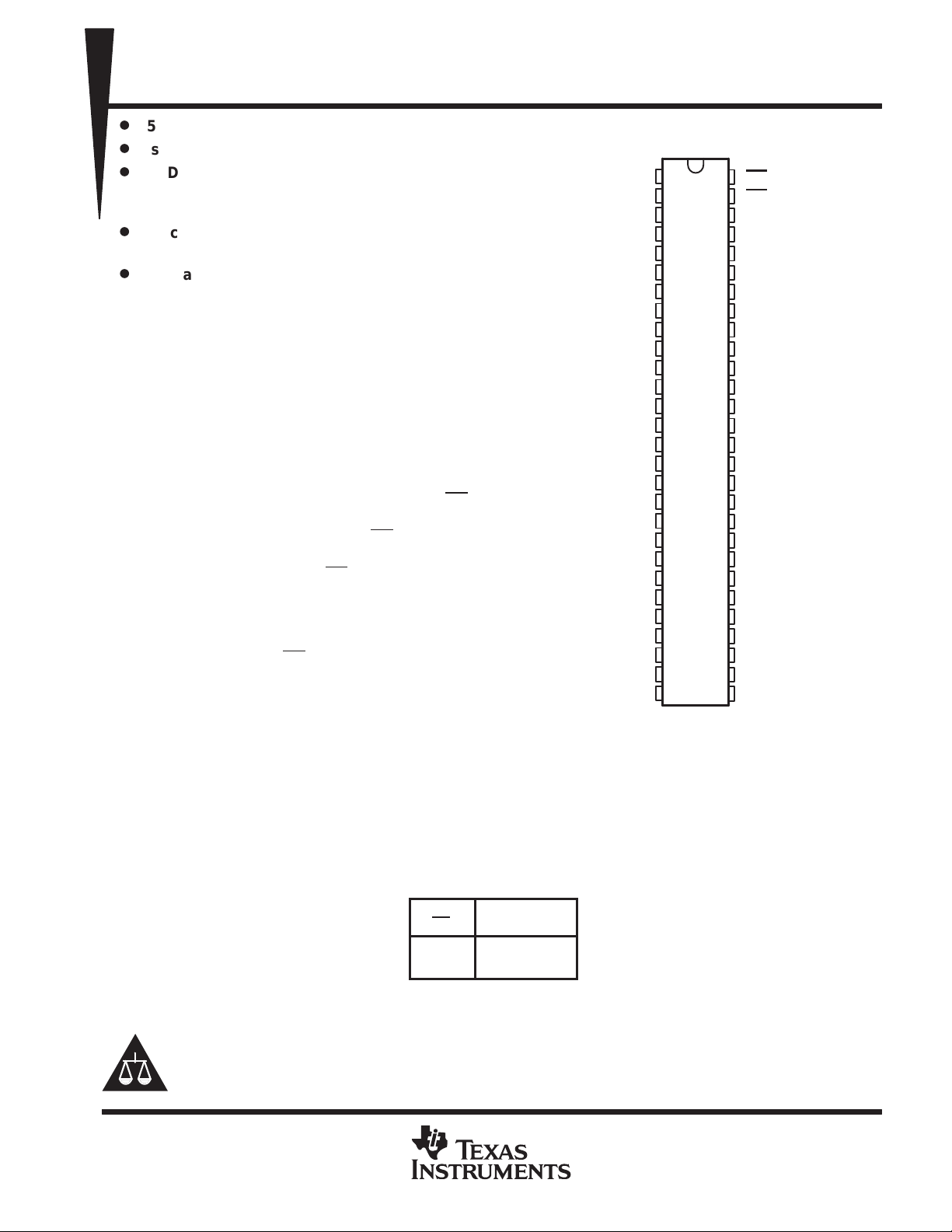
DGG, DGV, OR DL PACKAGE
)
(TOP VIEW)
1
2
3
4
5
6
7
8
9
10
11
12
13
14
15
16
17
18
19
20
21
22
23
24
25
26
27
28
56
55
54
53
52
51
50
49
48
47
46
45
44
43
42
41
40
39
38
37
36
35
34
33
32
31
30
29
1OE
2OE
1B1
1B2
1B3
1B4
1B5
GND
1B6
1B7
1B8
1B9
1B10
1B1 1
1B12
2B1
2B2
2B3
GND
2B4
2B5
2B6
2B7
2B8
2B9
2B10
2B1 1
2B12
NC
1A1
1A2
1A3
1A4
1A5
1A6
GND
1A7
1A8
1A9
1A10
1A1 1
1A12
2A1
2A2
V
CC
2A3
GND
2A4
2A5
2A6
2A7
2A8
2A9
2A10
2A1 1
2A12
NC – No internal connection
Please be aware that an important notice concerning availability, standard warranty, and use in critical applications of
Texas Instruments semiconductor products and disclaimers thereto appears at the end of this data sheet.
PRODUCTION DATA information is current as of publication date.
Products conform to specifications per the terms of Texas Instruments
standard warranty. Production processing does not necessarily include
testing of all parameters.
FUNCTION TABLE
(each 12-bit bus switch)
INPUT
OE
L A port = B port
H Disconnect
POST OFFICE BOX 655303 • DALLAS, TEXAS 75265
FUNCTION
Copyright 1999, Texas Instruments Incorporated
1
SN74CBTLV16211
LOW-VOLTAGE 24-BIT FET BUS SWITCH
SCDS043E – DECEMBER 1997 – REVISED APRIL 1999
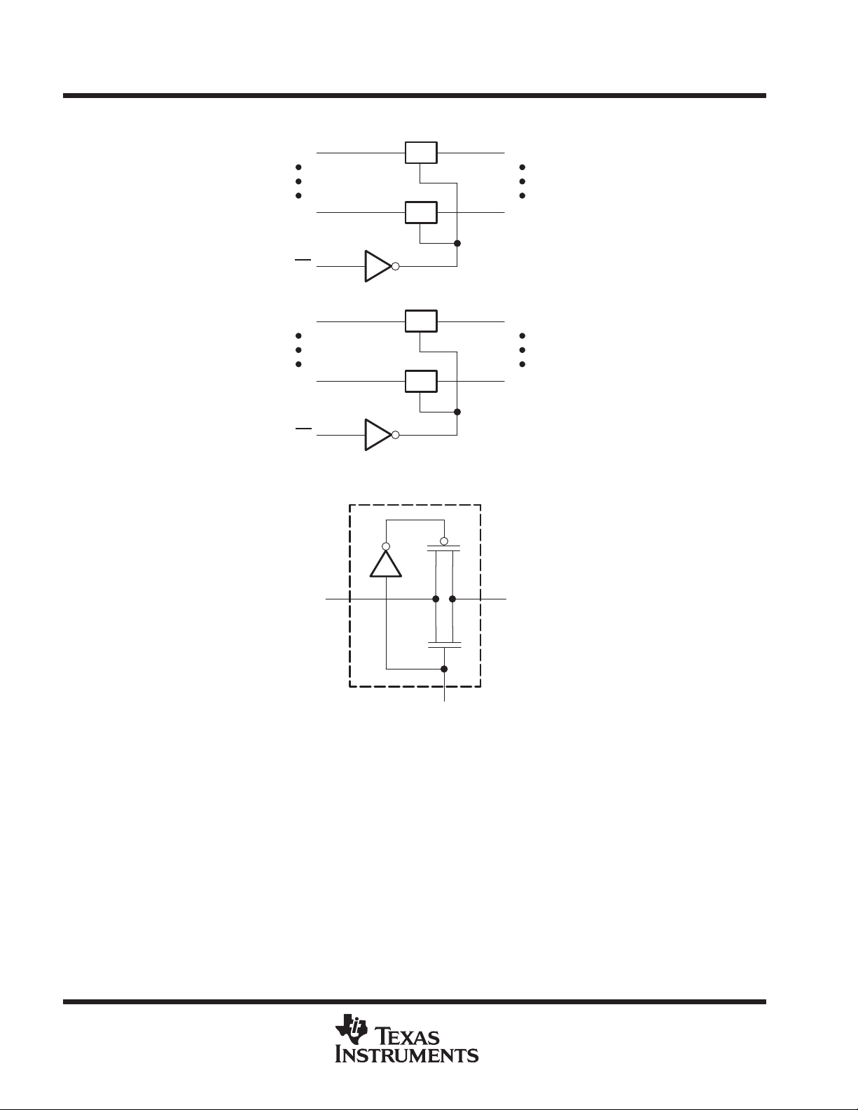
logic diagram (positive logic)
2
1A1
14
1A12
56
1OE
15
2A1
28
2A12
55
2OE
simplified schematic, each FET switch
SW
SW
SW
SW
54
42
41
29
1B1
1B12
2B1
2B12
A
(OE)
B
absolute maximum ratings over operating free-air temperature range (unless otherwise noted)
Supply voltage range, V
Input voltage range, V
Continuous channel current 128 mA. . . . . . . . . . . . . . . . . . . . . . . . . . . . . . . . . . . . . . . . . . . . . . . . . . . . . . . . . . . . . .
Input clamp current, I
Package thermal impedance, θ
Storage temperature range, T
†
Stresses beyond those listed under “absolute maximum ratings” may cause permanent damage to the device. These are stress ratings only, and
functional operation of the device at these or any other conditions beyond those indicated under “recommended operating conditions” is not
implied. Exposure to absolute-maximum-rated conditions for extended periods may affect device reliability.
NOTES: 1. The input and output negative-voltage ratings may be exceeded if the input and output clamp-current ratings are observed.
2. The package thermal impedance is calculated in accordance with JESD 51.
–0.5 V to 4.6 V. . . . . . . . . . . . . . . . . . . . . . . . . . . . . . . . . . . . . . . . . . . . . . . . . . . . . . . . .
CC
(see Note 1) –0.5 V to 4.6 V. . . . . . . . . . . . . . . . . . . . . . . . . . . . . . . . . . . . . . . . . . . . . . . . .
I
(V
< 0) –50 mA. . . . . . . . . . . . . . . . . . . . . . . . . . . . . . . . . . . . . . . . . . . . . . . . . . . . . . . . . . .
IK
I
(see Note 2): DGG package 81°C/W. . . . . . . . . . . . . . . . . . . . . . . . . . . . . . . .
JA
DGV package 86°C/W. . . . . . . . . . . . . . . . . . . . . . . . . . . . . . . .
DL package 74°C/W. . . . . . . . . . . . . . . . . . . . . . . . . . . . . . . . . .
–65°C to 150°C. . . . . . . . . . . . . . . . . . . . . . . . . . . . . . . . . . . . . . . . . . . . . . . . . . .
stg
†
2
POST OFFICE BOX 655303 • DALLAS, TEXAS 75265
 Loading...