

SN74CBTD1G125
SINGLE FET BUS SWITCH
WITH LEVEL SHIFTING
SCDS063C – JULY 1998 – REVISED OCT OBER 1999
1
POST OFFICE BOX 655303 • DALLAS, TEXAS 75265
D
5-Ω Switch Connection Between Two Ports
D
TTL-Compatible Control Input Levels
D
ESD Protection Exceeds 2000 V Per
MIL-STD-883, Method 3015; Exceeds 200 V
Using Machine Model (C = 200 pF, R = 0)
D
Latch-Up Performance Exceeds 100 mA Per
JESD 78, Class II
D
Packaged in Plastic Small-Outline
Transistor (DBV, DCK) Packages
description
The SN74CBTD1G125 features a single high-speed line switch. The switch is disabled when the output-enable
(OE) input is high. A diode to VCC is integrated on the chip to allow for level shifting between 5-V inputs and 3.3-V
outputs.
The SN74CBTD1G125 is characterized for operation from –40°C to 85°C.
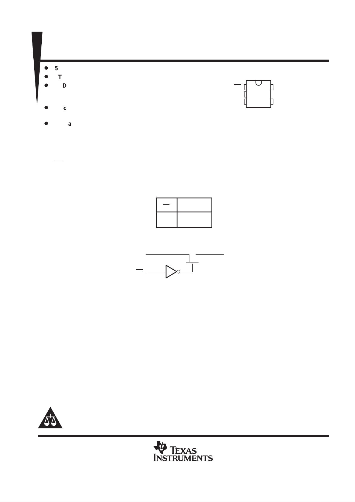
FUNCTION TABLE
INPUT
OE
FUNCTION
L A port = B port
H Disconnect
logic diagram (positive logic)
OE
B
A
2
1
4
DBV OR DCK PACKAGE
(TOP VIEW)
1
2
3
5
4
OE
A
GND
V
CC
B
PRODUCTION DATA information is current as of publication date.
Products conform to specifications per the terms of Texas Instruments
standard warranty. Production processing does not necessarily include
testing of all parameters.
Copyright 1999, Texas Instruments Incorporated
Please be aware that an important notice concerning availability, standard warranty, and use in critical applications of
Texas Instruments semiconductor products and disclaimers thereto appears at the end of this data sheet.
SN74CBTD1G125
SINGLE FET BUS SWITCH
WITH LEVEL SHIFTING
SCDS063C – JULY 1998 – REVISED OCT OBER 1999
2
POST OFFICE BOX 655303 • DALLAS, TEXAS 75265
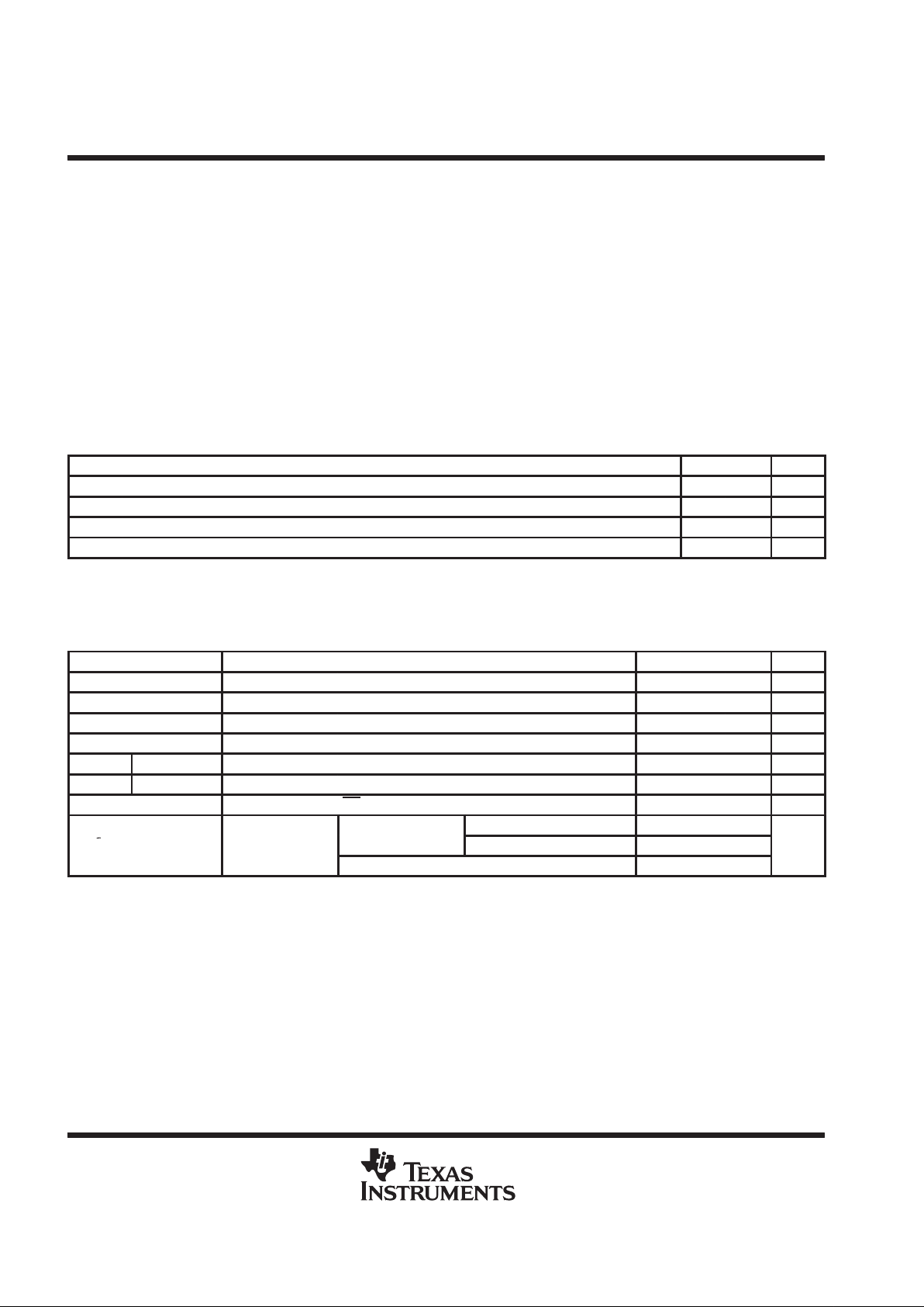
absolute maximum ratings over operating free-air temperature range (unless otherwise noted)
†
Supply voltage range, VCC –0.5 V to 7 V. . . . . . . . . . . . . . . . . . . . . . . . . . . . . . . . . . . . . . . . . . . . . . . . . . . . . . . . . .
Input voltage range, VI (see Note 1) –0.5 V to 7 V. . . . . . . . . . . . . . . . . . . . . . . . . . . . . . . . . . . . . . . . . . . . . . . . . .
Continuous channel current 128 mA. . . . . . . . . . . . . . . . . . . . . . . . . . . . . . . . . . . . . . . . . . . . . . . . . . . . . . . . . . . . . .
Input clamp current, I
IK
(V
I/O
< 0) –50 mA. . . . . . . . . . . . . . . . . . . . . . . . . . . . . . . . . . . . . . . . . . . . . . . . . . . . . . . . .
Package thermal impedance, θJA (see Note 2): DBV package 347°C/W. . . . . . . . . . . . . . . . . . . . . . . . . . . . . . .
DCK package 389°C/W. . . . . . . . . . . . . . . . . . . . . . . . . . . . . . .
Storage temperature range, T
stg
–65°C to 150°C. . . . . . . . . . . . . . . . . . . . . . . . . . . . . . . . . . . . . . . . . . . . . . . . . . .
†
Stresses beyond those listed under “absolute maximum ratings” may cause permanent damage to the device. These are stress ratings only, and
functional operation of the device at these or any other conditions beyond those indicated under “recommended operating conditions” is not
implied. Exposure to absolute-maximum-rated conditions for extended periods may affect device reliability.
NOTES: 1. The input and output negative-voltage ratings may be exceeded if the input and output clamp-current ratings are observed.
2. The package thermal impedance is calculated in accordance with JESD 51.
recommended operating conditions (see Note 3)
MIN MAX UNIT
V
CC
Supply voltage 4.5 5.5 V
V
IH
High-level control input voltage 2 V
V
IL
Low-level control input voltage 0.8 V
T
A
Operating free-air temperature –40 85 °C
NOTE 3: All unused control inputs of the device must be held at VCC or GND to ensure proper device operation. Refer to the TI application report,
Implications of Slow or Floating CMOS Inputs
, literature number SCBA004.
electrical characteristics over recommended operating free-air temperature range (unless
otherwise noted)
PARAMETER TEST CONDITIONS MIN TYP‡MAX UNIT
V
IK
VCC = 4.5 V, II = –18 mA –1.2 V
V
OH
See Figure 2
I
I
VCC = 5.5 V, VI = 5.5 V or GND ±1 µA
I
CC
VCC = 5.5 V, IO = 0, VI = VCC or GND 1.5 mA
∆I
CC
§
Control input VCC = 5.5 V, One input at 3.4 V , Other inputs at VCC or GND 2.5 mA
C
i
Control input VI = 3 V or 0 2 pF
C
io(OFF)
VO = 3 V or 0, OE = V
CC
3.5 pF
II = 64 mA 5 7
r
on
¶
VCC = 4.5 V
V
I
=
0
II = 30 mA 5 7
Ω
VI = 2.4 V, II = 15 mA 35 50
‡
All typical values are at VCC = 5 V, TA = 25°C.
§
This is the increase in supply current for each input that is at the specified TTL voltage level rather than VCC or GND.
¶
Measured by the voltage drop between the A and the B terminals at the indicated current through the switch. On-state resistance is determined
by the lower voltage of the two (A or B) terminals.
 Loading...