

Texas Instruments SN74CBT6800DGVR, SN74CBT6800DWR, SN74CBT6800PWLE, SN74CBT6800PWR, SN74CBT6800DBLE Datasheet
...
SN74CBT6800A
10-BIT FET BUS SWITCH
WITH PRECHARGED OUTPUTS
SCDS005L – MARCH 1993 – REVISED JUL Y 1999
1
POST OFFICE BOX 655303 • DALLAS, TEXAS 75265
D
5-Ω Switch Connection Between Two Ports
D
TTL-Compatible Input Levels
D
Outputs Are Precharged by Bias Voltage to
Minimize Signal Distortion During Live
Insertion
D
Package Options Include Plastic Shrink
Small-Outline (DB, DBQ), Small-Outline
(DW), and Thin Shrink Small-Outline (PW)
Packages
description
The SN74CBT6800A provides ten bits of
high-speed TTL-compatible bus switching. The
low on-state resistance of the switch allows
bidirectional connections to be made while adding
near-zero propagation delay. The device also
precharges the B port to a user-selectable bias
voltage (BIASV) to minimize live-insertion noise.
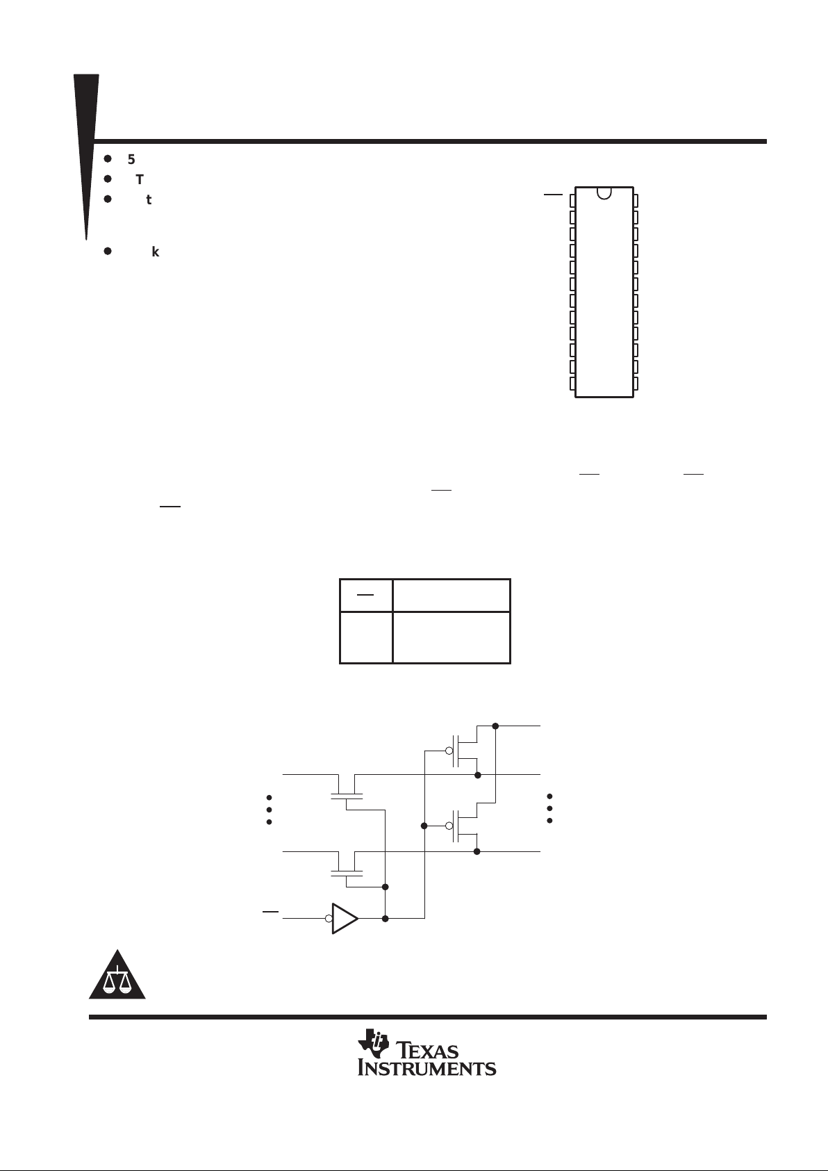
The SN74CBT6800A is organized as one 10-bit switch with a single enable (ON
) input. When ON is low, the
switch is on and port A is connected to port B. When ON
is high, the switch between port A and port B is open.
When ON
is high or VCC is 0 V, B port is precharged to BIASV through the equivalent of a 10-kΩ resistor.
The SN74CBT6800A is characterized for operation from –40°C to 85°C.
FUNCTION TABLE
INPUT
ON
FUNCTION
L A port = B port
H
A port = Z
B port = BIASV
logic diagram (positive logic)
ON
A1
A10
B1
BIASV
B10
2
11
1
13
23
14
DB, DBQ, DW, OR PW PACKAGE
(TOP VIEW)
ON
A1
A2
A3
A4
A5
A6
A7
A8
A9
A10
GND
V
CC
B1
B2
B3
B4
B5
B6
B7
B8
B9
B10
BIASV
1
2
3
4
5
6
7
8
9
10
11
12
24
23
22
21
20
19
18
17
16
15
14
13
PRODUCTION DATA information is current as of publication date.
Products conform to specifications per the terms of Texas Instruments
standard warranty. Production processing does not necessarily include
testing of all parameters.
Copyright 1999, Texas Instruments Incorporated
Please be aware that an important notice concerning availability, standard warranty, and use in critical applications of
Texas Instruments semiconductor products and disclaimers thereto appears at the end of this data sheet.
SN74CBT6800A
10-BIT FET BUS SWITCH
WITH PRECHARGED OUTPUTS
SCDS005L – MARCH 1993 – REVISED JUL Y 1999
2
POST OFFICE BOX 655303 • DALLAS, TEXAS 75265
absolute maximum ratings over operating free-air temperature range (unless otherwise noted)
†
Supply voltage range, V
CC
–0.5 V to 7 V. . . . . . . . . . . . . . . . . . . . . . . . . . . . . . . . . . . . . . . . . . . . . . . . . . . . . . . . . .
Bias voltage range, BIASV –0.5 V to 7 V. . . . . . . . . . . . . . . . . . . . . . . . . . . . . . . . . . . . . . . . . . . . . . . . . . . . . . . . . .
Input voltage range, V
I
(see Note 1) –0.5 V to 7 V. . . . . . . . . . . . . . . . . . . . . . . . . . . . . . . . . . . . . . . . . . . . . . . . . .
Continuous channel current 128 mA. . . . . . . . . . . . . . . . . . . . . . . . . . . . . . . . . . . . . . . . . . . . . . . . . . . . . . . . . . . . . .
Input clamp current, I
IK
(V
I
< 0) –50 mA. . . . . . . . . . . . . . . . . . . . . . . . . . . . . . . . . . . . . . . . . . . . . . . . . . . . . . . . . . .
Package thermal impedance, θ
JA
(see Note 2): DB package 104°C/W. . . . . . . . . . . . . . . . . . . . . . . . . . . . . . . .
DBQ package 103°C/W. . . . . . . . . . . . . . . . . . . . . . . . . . . . . . .
DW package 81°C/W. . . . . . . . . . . . . . . . . . . . . . . . . . . . . . . . .
PW package 120°C/W. . . . . . . . . . . . . . . . . . . . . . . . . . . . . . . .
Storage temperature range, T
stg
–65°C to 150°C. . . . . . . . . . . . . . . . . . . . . . . . . . . . . . . . . . . . . . . . . . . . . . . . . . .
†
Stresses beyond those listed under “absolute maximum ratings” may cause permanent damage to the device. These are stress ratings only, and
functional operation of the device at these or any other conditions beyond those indicated under “recommended operating conditions” is not
implied. Exposure to absolute-maximum-rated conditions for extended periods may affect device reliability.
NOTES: 1. The input and output negative-voltage ratings may be exceeded if the input and output clamp-current ratings are observed.
2. The package thermal impedance is calculated in accordance with JESD 51.
recommended operating conditions (see Note 3)
MIN MAX UNIT
V
CC
Supply voltage 4 5.5 V
BIASV Supply voltage 1.3 V
CC
V
V
IH
High-level control input voltage 2 V
V
IL
Low-level control input voltage 0.8 V
T
A
Operating free-air temperature –40 85 °C
NOTE 3: All unused control inputs of the device must be held at VCC or GND to ensure proper device operation. Refer to the TI application report,
Implications of Slow or Floating CMOS Inputs
, literature number SCBA004.
electrical characteristics over recommended operating free-air temperature range (unless
otherwise noted)
PARAMETER TEST CONDITIONS MIN TYP‡MAX UNIT
V
IK
VCC = 4.5 V, II = –18 mA –1.2 V
I
I
VCC = 5.5 V, VI = 5.5 V or GND ±5 µA
I
O
VCC = 4.5 V, BIASV = 2.4 V , VO= 0 0.25 mA
I
CC
VCC = 5.5 V, IO = 0, VI = VCC or GND 50 µA
∆I
CC
§
Control inputs VCC = 5.5 V, One input at 3.4 V , Other inputs at VCC or GND 2.5 mA
C
i
Control inputs VI = 3 V or 0 3.5 pF
C
o(OFF)
VO = 3 V or 0, Switch off 4.5 pF
VCC = 4 V,
TYP at VCC = 4 V
VI = 2.4 V, II = 15 mA 11 20
r
¶
II = 64 mA 3 7
Ω
on
VCC = 4.5 V
V
I
=
0
II = 30 mA 3 7
VI = 2.4 V, II = 15 mA 6 15
‡
All typical values are at VCC = 5 V (unless otherwise noted), TA = 25°C.
§
This is the increase in supply current for each input that is at the specified TTL voltage level rather than VCC or GND.
¶
Measured by the voltage drop between the A and B terminals at the indicated current through the switch. On-state resistance is determined by
the lower of the voltages of the two (A or B) terminals.
 Loading...