

Texas Instruments SN74CBT3251DR, SN74CBT3251PWLE, SN74CBT3251PWR, SN74CBT3251D, SN74CBT3251DBLE Datasheet
...
FUNCTION
SN74CBT3251
1-OF-8 FET MULTIPLEXER/DEMULTIPLEXER
SCDS019G – MAY 1995 – REVISED MAY 1998
D
Functionally Equivalent to QS3251
D
5-Ω Switch Connection Between Two Ports
D
TTL-Compatible Input Levels
D
Package Options Include Plastic
Small-Outline (D), Shrink Small-Outline
(DB, DBQ), Thin Very Small-Outline (DGV),
and Thin Shrink Small-Outline (PW)
Packages
description
The SN74CBT3251 is a 1-of-8 high-speed
TTL-compatible FET multiplexer/demultiplexer.
The low on-state resistance of the switch allows
connections to be made with minimal propagation
delay .
When output enable (OE
the A-input data.
The SN74CBT3251 is characterized for operation from –40°C to 85°C.
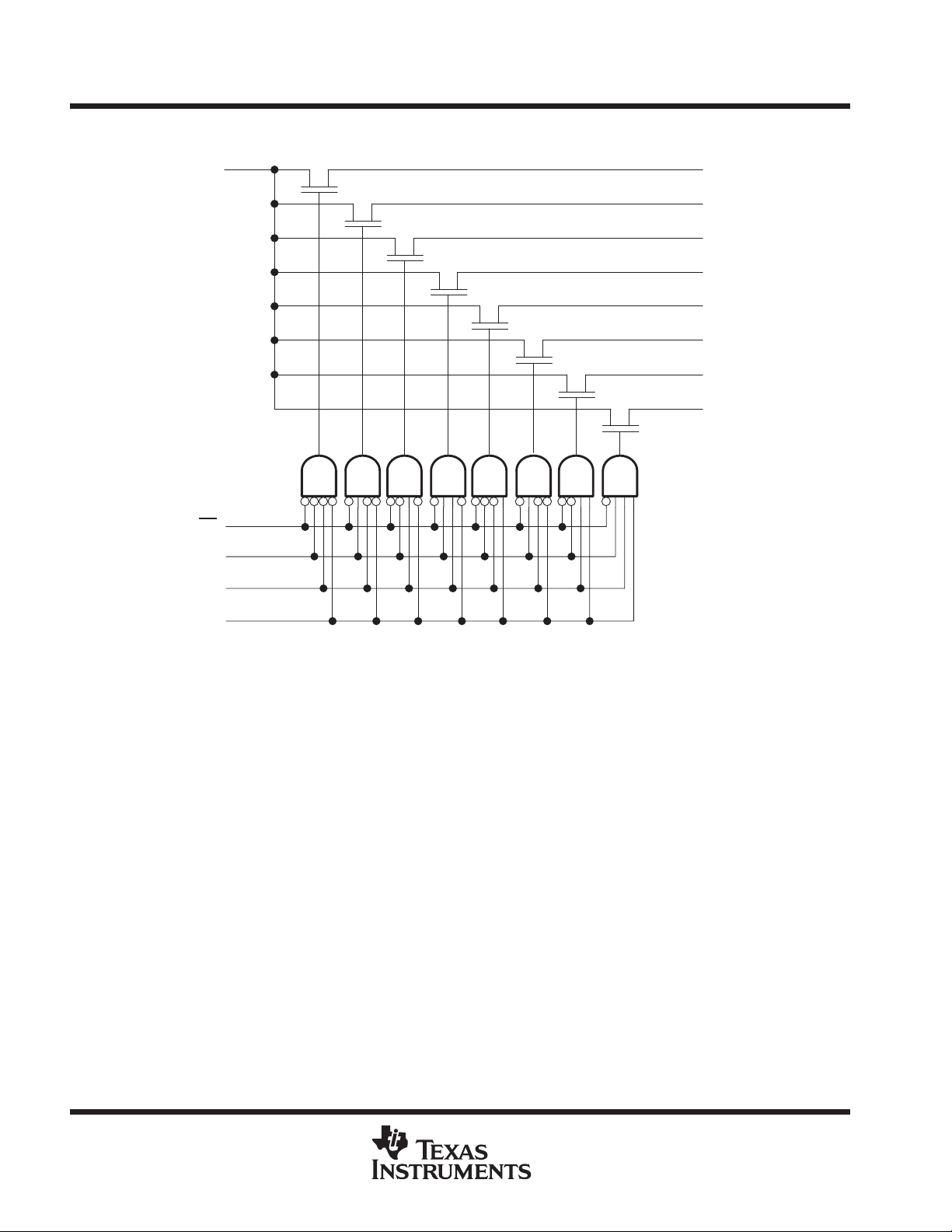
) is low, the SN74CBT3251 is enabled. S0, S1, and S2 select one of the B outputs for
FUNCTION TABLE
(each multiplexer/demultiplexer)
INPUTS
OE S2 S1 S0
L L L L A port = B1 port
L L L H A port = B2 port
L L H L A port = B3 port
L L H H A port = B4 port
L H L L A port = B5 port
L H L H A port = B6 port
L H H L A port = B7 port
L H H H A port = B8 port
H X X X Disconnect
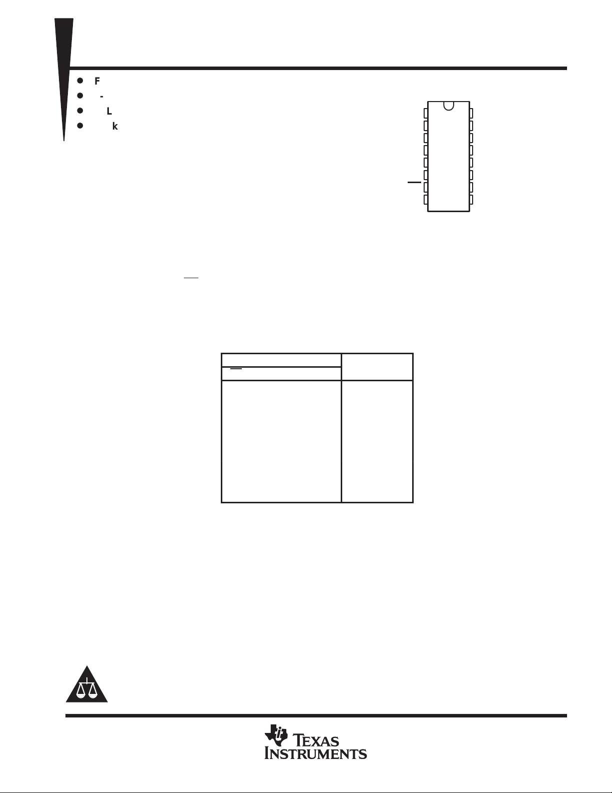
D, DB, DBQ, DGV, OR PW PACKAGE
(TOP VIEW)
16
15
14
13
12
11
10
V
CC
B5
B6
B7
B8
S0
S1
9
S2
1
B4
2
B3
3
B2
4
B1
5
A
6
NC
7
OE
8
GND
NC – No internal connection
Please be aware that an important notice concerning availability, standard warranty, and use in critical applications of
Texas Instruments semiconductor products and disclaimers thereto appears at the end of this data sheet.
PRODUCTION DATA information is current as of publication date.
Products conform to specifications per the terms of Texas Instruments
standard warranty. Production processing does not necessarily include
testing of all parameters.
POST OFFICE BOX 655303 • DALLAS, TEXAS 75265
Copyright 1998, Texas Instruments Incorporated
1
SN74CBT3251
1-OF-8 FET MULTIPLEXER/DEMULTIPLEXER
SCDS019G – MAY 1995 – REVISED MAY 1998
logic diagram (positive logic)
OE
S0
S1
S2
15
14
13
12
4
B1
3
B2
2
B3
1
B4
B5
B6
B7
B8
5
A
7
11
10
9
absolute maximum ratings over operating free-air temperature range (unless otherwise noted)
Supply voltage range, V
Input voltage range, V
Continuous channel current 128 mA. . . . . . . . . . . . . . . . . . . . . . . . . . . . . . . . . . . . . . . . . . . . . . . . . . . . . . . . . . . . . .
Input clamp current, I
Package thermal impedance, θ
Storage temperature range, T
†
Stresses beyond those listed under “absolute maximum ratings” may cause permanent damage to the device. These are stress ratings only, and
functional operation of the device at these or any other conditions beyond those indicated under “recommended operating conditions” is not
implied. Exposure to absolute-maximum-rated conditions for extended periods may affect device reliability.
NOTES: 1. The input and output negative-voltage ratings may be exceeded if the input and output clamp-current ratings are observed.
2. The package thermal impedance is calculated in accordance with JESD 51.
–0.5 V to 7 V. . . . . . . . . . . . . . . . . . . . . . . . . . . . . . . . . . . . . . . . . . . . . . . . . . . . . . . . . .
CC
(see Note 1) –0.5 V to 7 V. . . . . . . . . . . . . . . . . . . . . . . . . . . . . . . . . . . . . . . . . . . . . . . . . .
I
(V
< 0) –50 mA. . . . . . . . . . . . . . . . . . . . . . . . . . . . . . . . . . . . . . . . . . . . . . . . . . . . . . . . . .
I/O
(see Note 2): D package 113°C/W. . . . . . . . . . . . . . . . . . . . . . . . . . . . . . . . . .
JA
K
DB package 131°C/W. . . . . . . . . . . . . . . . . . . . . . . . . . . . . . . . .
DBQ package 139°C/W. . . . . . . . . . . . . . . . . . . . . . . . . . . . . . .
DGV package 180°C/W. . . . . . . . . . . . . . . . . . . . . . . . . . . . . . .
PW package 149°C/W. . . . . . . . . . . . . . . . . . . . . . . . . . . . . . . .
–65°C to 150°C. . . . . . . . . . . . . . . . . . . . . . . . . . . . . . . . . . . . . . . . . . . . . . . . . . .
stg
†
2
POST OFFICE BOX 655303 • DALLAS, TEXAS 75265
 Loading...