

SN74CBT16861
20-BIT FET BUS SWITCH
SCDS068A – JULY 1998 – REVISED DECEMBER 1999
D
5-Ω Switch Connection Between Two Ports
D
TTL-Compatible Input Levels
D
Latch-Up Performance Exceeds 100 mA Per
JESD 78, Class II
D
Package Options Include Plastic Thin
Shrink Small-Outline (DGG) and Shrink
Small-Outline (DL) Packages
description
The SN74CBT16861 provides 20 bits of
high-speed TTL-compatible bus switching. The
low on-state resistance of the switch allows
connections to be made with minimal propagation
delay .
The device is organized as one dual 10-bit switch
with separate output-enable (OE) input. When OE
is low, the switch is on, and port A is connected to
port B. When OE is high, the switch is open, and
the high-impedance state exists between the two
ports.
The SN74CBT16861 is characterized for
operation from –40°C to 85°C.
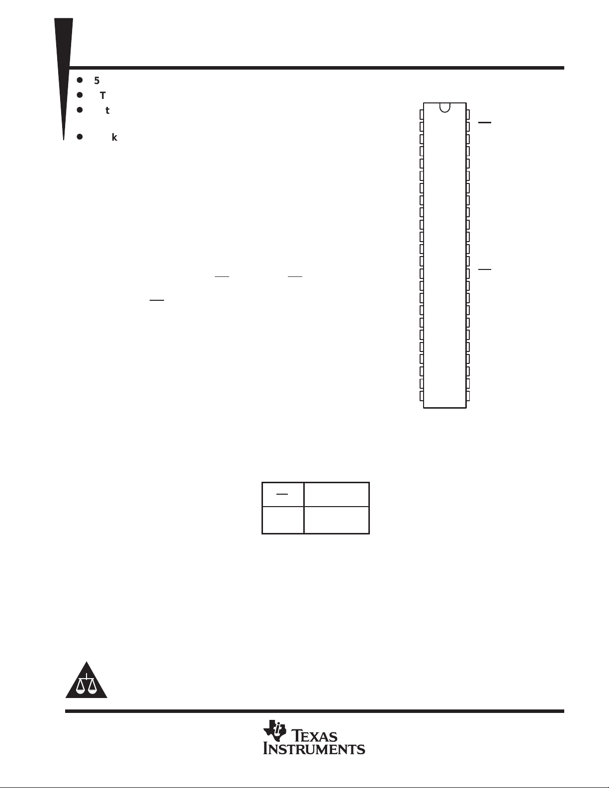
DGG OR DL PACKAGE
(TOP VIEW)
1
2
3
4
5
6
7
8
9
10
11
12
13
14
15
16
17
18
19
20
21
22
23
24
48
47
46
45
44
43
42
41
40
39
38
37
36
35
34
33
32
31
30
29
28
27
26
25
NC
1A1
1A2
1A3
1A4
1A5
1A6
1A7
1A8
1A9
1A10
GND
NC
2A1
2A2
2A3
2A4
2A5
2A6
2A7
2A8
2A9
2A10
GND
V
CC
1OE
1B1
1B2
1B3
1B4
1B5
1B6
1B7
1B8
1B9
1B10
V
CC
2OE
2B1
2B2
2B3
2B4
2B5
2B6
2B7
2B8
2B9
2B10
NC – No internal connection
FUNCTION TABLE
(each 10-bit bus switch)
INPUT
OE
L A port = B port
H Disconnect
Please be aware that an important notice concerning availability, standard warranty, and use in critical applications of
Texas Instruments semiconductor products and disclaimers thereto appears at the end of this data sheet.
FUNCTION
PRODUCTION DATA information is current as of publication date.
Products conform to specifications per the terms of Texas Instruments
standard warranty. Production processing does not necessarily include
testing of all parameters.
POST OFFICE BOX 655303 • DALLAS, TEXAS 75265
Copyright 1999, Texas Instruments Incorporated
1
SN74CBT16861
20-BIT FET BUS SWITCH
SCDS068A – JULY 1998 – REVISED DECEMBER 1999
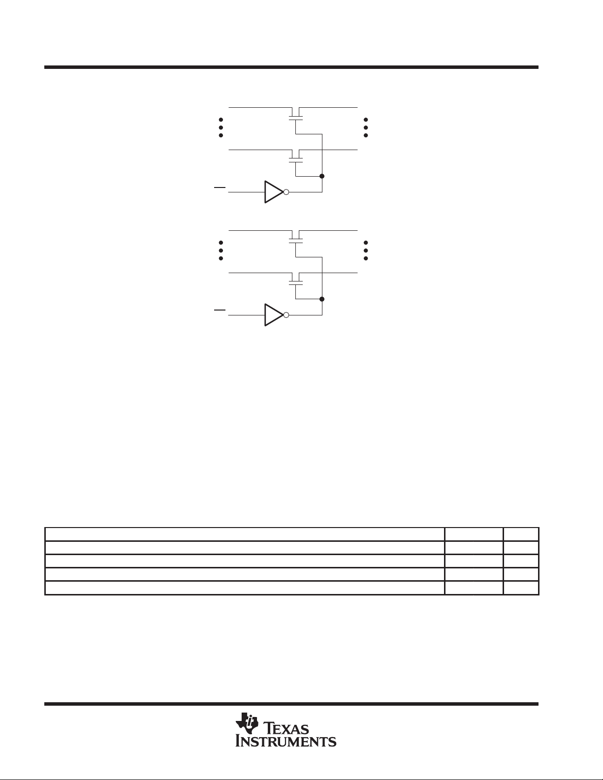
logic diagram (positive logic)
1A1
1A10
1OE
2A1
2A10
2OE
2
11
47
14
23
35
46
37
34
25
1B1
1B10
2B1
2B10
absolute maximum ratings over operating free-air temperature range (unless otherwise noted)
Supply voltage range, V
Input voltage range, VI (see Note 1) –0.5 V to 7 V. . . . . . . . . . . . . . . . . . . . . . . . . . . . . . . . . . . . . . . . . . . . . . . . . .
Continuous channel current 128 mA. . . . . . . . . . . . . . . . . . . . . . . . . . . . . . . . . . . . . . . . . . . . . . . . . . . . . . . . . . . . . .
Input clamp current, I
Package thermal impedance, θJA (see Note 2): DGG package 70°C/W. . . . . . . . . . . . . . . . . . . . . . . . . . . . . . .
Storage temperature range, T
†
Stresses beyond those listed under “absolute maximum ratings” may cause permanent damage to the device. These are stress ratings only, and
functional operation of the device at these or any other conditions beyond those indicated under “recommended operating conditions” is not
implied. Exposure to absolute-maximum-rated conditions for extended periods may affect device reliability.
NOTES: 1. The input and output negative-voltage ratings may be exceeded if the input and output clamp-current ratings are observed.
2. The package thermal impedance is calculated in accordance with JESD 51.
–0.5 V to 7 V. . . . . . . . . . . . . . . . . . . . . . . . . . . . . . . . . . . . . . . . . . . . . . . . . . . . . . . . . .
CC
(V
< 0) –50 mA. . . . . . . . . . . . . . . . . . . . . . . . . . . . . . . . . . . . . . . . . . . . . . . . . . . . . . . . .
I/O
IK
DL package 63°C/W. . . . . . . . . . . . . . . . . . . . . . . . . . . . . . . . .
–65°C to 150°C. . . . . . . . . . . . . . . . . . . . . . . . . . . . . . . . . . . . . . . . . . . . . . . . . . .
stg
†
recommended operating conditions (see Note 3)
MIN MAX UNIT
V
V
V
T
NOTE 3: All unused control inputs of the device must be held at VCC or GND to ensure proper device operation. Refer to the TI application report,
2
Supply voltage 4 5.5 V
CC
High-level control input voltage 2 V
IH
Low-level control input voltage 0.8 V
IL
Operating free-air temperature –40 85 °C
A
Implications of Slow or Floating CMOS Inputs
, literature number SCBA004.
POST OFFICE BOX 655303 • DALLAS, TEXAS 75265
 Loading...