

Texas Instruments SN74CBT16212ADGGR, SN74CBT16212ADGVR, SN74CBT16212ADL, SN74CBT16212ADLR, SNJ54CBT16212AWD Datasheet
FUNCTION
SN54CBT16212A, SN74CBT16212A
24-BIT FET BUS-EXCHANGE SWITCHES
SCDS007M – NOVEMBER 1992 – REVISED SEPTEMBER 1998
D
5-Ω Switch Connection Between Two Ports
D
TTL-Compatible Input Levels
D
Latch-Up Performance Exceeds 250 mA Per
JESD 17
D
ESD Protection Exceeds 2000 V Per
MIL-STD-833, Method 3015; Exceeds 200 V
Using Machine Model (C = 200 pF, R = 0)
D
Package Options Include Plastic Thin
Shrink Small-Outline (DGG), Thin Very
Small-Outline (DGV), and Shrink
Small-Outline (DL) Packages, and Ceramic
Flat (WD) Package
description
The ’CBT16212A devices provide 24 bits of
high-speed TTL-compatible bus switching or
exchanging. The low on-state resistance of the
switch allows connections to be made with
minimal propagation delay.
Each device operates as a 24-bit bus switch or a
12-bit bus exchanger, which provides data
exchanging between the four signal ports via the
data-select (S0, S1, S2) terminals.
The SN54CBT16212A is characterized for
operation over the full military temperature range
of –55°C to 125°C. The SN74CBT16212A is
characterized for operation from –40°C to 85°C.
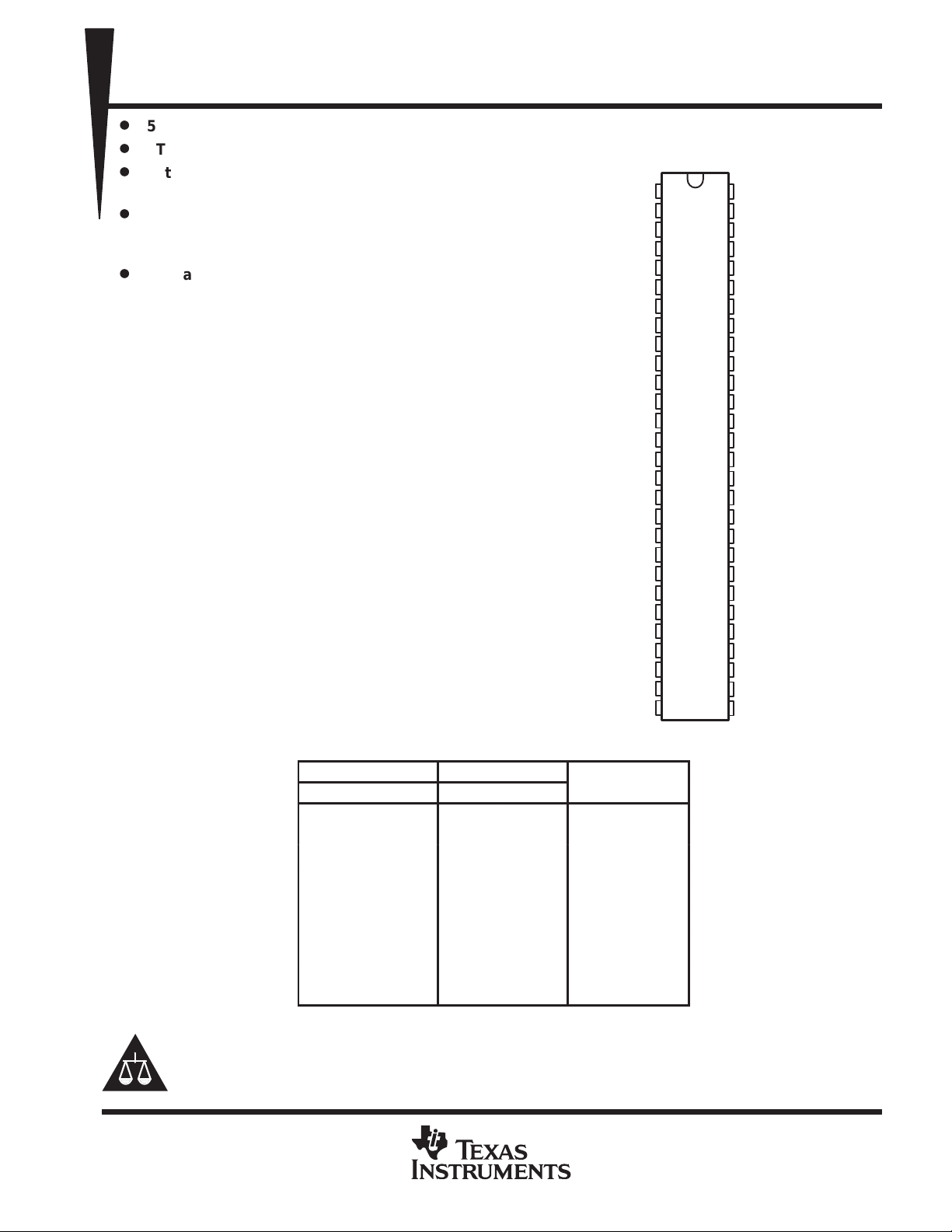
SN54CBT16212A ...WD PACKAGE
SN74CBT16212A . . . DGG, DGV, OR DL PACKAGE
S0
1A1
1A2
2A1
2A2
3A1
3A2
GND
4A1
4A2
5A1
5A2
6A1
6A2
7A1
7A2
V
CC
8A1
GND
8A2
9A1
9A2
10A1
10A2
1 1A1
1 1A2
12A1
12A2
(TOP VIEW)
1
56
2
55
3
54
4
53
5
52
6
51
7
50
8
49
9
48
10
47
11
46
12
45
13
44
14
43
15
42
16
41
17
40
18
39
19
38
20
37
21
36
22
35
23
34
24
33
25
32
26
31
27
30
28
29
S1
S2
1B1
1B2
2B1
2B2
3B1
GND
3B2
4B1
4B2
5B1
5B2
6B1
6B2
7B1
7B2
8B1
GND
8B2
9B1
9B2
10B1
10B2
1 1B1
1 1B2
12B1
12B2
INPUTS
S2 S1 S0 A1 A2
L L L Z Z Disconnect
L L H B1 port Z A1 port = B1 port
L H L B2 port Z A1 port = B2 port
L HH Z B1 port A2 port = B1 port
H LL ZB2 port A2 port = B2 port
H LH Z Z Disconnect
H H L B1 port B2 port
H H H B2 port B1 port
Please be aware that an important notice concerning availability, standard warranty, and use in critical applications of
Texas Instruments semiconductor products and disclaimers thereto appears at the end of this data sheet.
PRODUCTION DATA information is current as of publication date.
Products conform to specifications per the terms of Texas Instruments
standard warranty. Production processing does not necessarily include
testing of all parameters.
FUNCTION TABLE
INPUTS/OUTPUTS
A1 port = B1 port
A2 port = B2 port
A1 port = B2 port
A2 port = B1 port
POST OFFICE BOX 655303 • DALLAS, TEXAS 75265
Copyright 1998, Texas Instruments Incorporated
On products compliant to MIL-PRF-38535, all parameters are tested
unless otherwise noted. On all other products, production
processing does not necessarily include testing of all parameters.
1
SN54CBT16212A, SN74CBT16212A
24-BIT FET BUS-EXCHANGE SWITCHES
SCDS007M – NOVEMBER 1992 – REVISED SEPTEMBER 1998
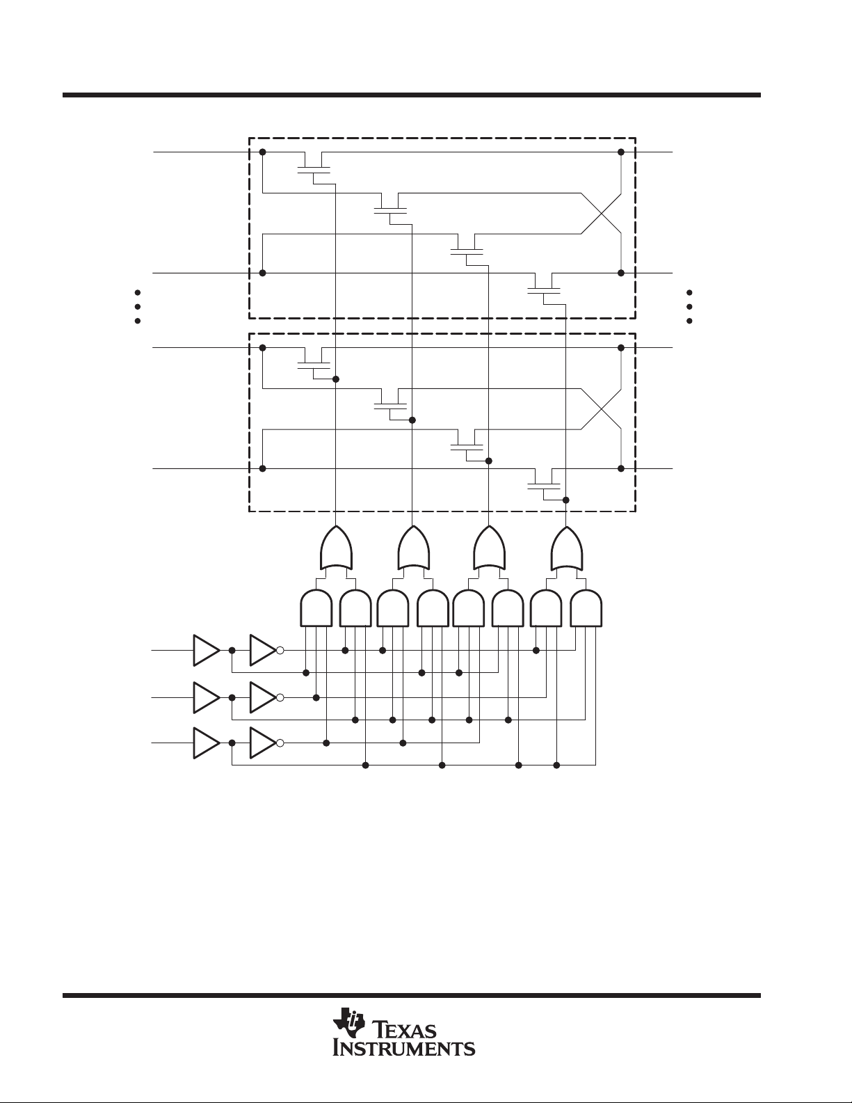
logic diagram (positive logic)
1A1
1A2
12A1
12A2
2
3
27
28
54
53
30
29
1B1
1B2
12B1
12B2
1
S0
56
S1
55
S2
Pin numbers shown are for the DGG, DGV, and DL packages.
2
POST OFFICE BOX 655303 • DALLAS, TEXAS 75265
 Loading...