

Texas Instruments SN74BCT756DW, SN74BCT756DWR, SN74BCT756N Datasheet
SN74BCT756
OCTAL BUFFER/DRIVER
WITH OPEN-COLLECTOR OUTPUTS
SCBS056B – OCTOBER 1990 – REVISED JUL Y 1997
1
POST OFFICE BOX 655303 • DALLAS, TEXAS 75265
D
BiCMOS Design Significantly Reduces I
CCZ
D
ESD Protection Exceeds 2000 V Per
MIL-STD-883, Method 3015; Exceeds 200 V
Using Machine Model (C = 200 pF, R = 0)
D
Open-Collector Outputs Drive Bus Lines or
Buffer Memory Address Registers
D
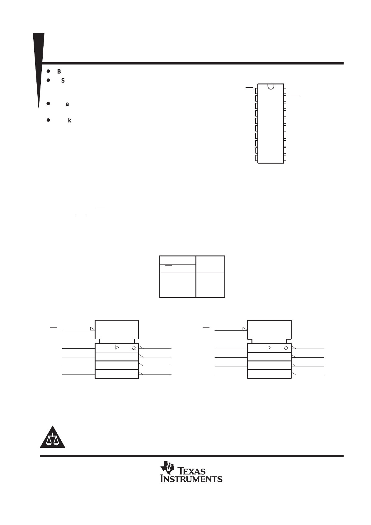
Package Options Include Plastic
Small-Outline Packages (DW) and Standard
Plastic 300-mil DIPs (N)
description
This octal buffer and line driver is designed
specifically to improve both the performance and
density of 3-state memory address drivers, clock
drivers, and bus-oriented receivers and
transmitters. The SN74BCT756, SN74BCT757,
and SN74BCT760 provide the choice of selected
combinations of inverting outputs, symmetrical
output-enable (OE
) inputs, and complementary
OE and OE inputs.
The SN74BCT756 is characterized for operation
from 0°C to 70°C.
FUNCTION TABLE
INPUTS
OUTPUT
OE A
Y
H X H
L LH
L H L
logic symbol
†
2
1A1
4
1A2
6
1A3
8
1A4
EN
1
1Y1
18
1Y2
16
1Y3
14
1Y4
12
11
2A1
13
2A2
15
2A3
17
2A4
EN
19
2Y1
9
2Y2
7
2Y3
5
2Y4
3
1OE 2OE
†
This symbol is in accordance with ANSI/IEEE Std 91-1984 and IEC Publication 617-12.
Copyright 1997, Texas Instruments Incorporated
PRODUCTION DATA information is current as of publication date.
Products conform to specifications per the terms of Texas Instruments
standard warranty. Production processing does not necessarily include
testing of all parameters.
Please be aware that an important notice concerning availability, standard warranty, and use in critical applications of
Texas Instruments semiconductor products and disclaimers thereto appears at the end of this data sheet.
1
2
3
4
5
6
7
8
9
10
20
19
18
17
16
15
14
13
12
11
1OE
1A1
2Y4
1A2
2Y3
1A3
2Y2
1A4
2Y1
GND
V
CC
2OE
1Y1
2A4
1Y2
2A3
1Y3
2A2
1Y4
2A1
DW OR N PACKAGE
(TOP VIEW)
SN74BCT756
OCTAL BUFFER/DRIVER
WITH OPEN-COLLECTOR OUTPUTS
SCBS056B – OCTOBER 1990 – REVISED JUL Y 1997
2
POST OFFICE BOX 655303 • DALLAS, TEXAS 75265
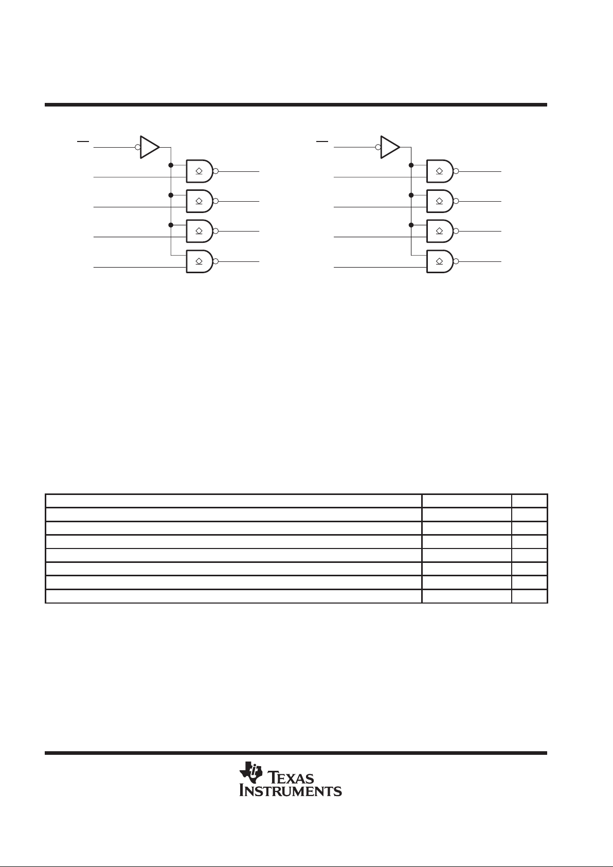
logic diagram (positive logic)
1
2
18
1OE
1A1
1Y1
4
16
1A2
1Y2
6
14
1A3
1Y3
8
12
1A4
1Y4
19
11
9
2OE
2A1
2Y1
13
7
2A2
2Y2
15
5
2A3
2Y3
17
3
2A4
2Y4
absolute maximum ratings over operating free-air temperature range (unless otherwise noted)
†
Supply voltage range, V
CC
–0.5 V to 7 V. . . . . . . . . . . . . . . . . . . . . . . . . . . . . . . . . . . . . . . . . . . . . . . . . . . . . . . . . .
Input voltage range, V
I
–0.5 V to 7 V. . . . . . . . . . . . . . . . . . . . . . . . . . . . . . . . . . . . . . . . . . . . . . . . . . . . . . . . . . . . . .
Input current range, I
I
–30 mA to 5 mA. . . . . . . . . . . . . . . . . . . . . . . . . . . . . . . . . . . . . . . . . . . . . . . . . . . . . . . . . . . . .
Voltage range applied to any output in the disabled or power-off state, VO –0.5 V to 5.5 V. . . . . . . . . . . . . . . .
Voltage range applied to any output in the high state, VO –0.5 V to V
CC
. . . . . . . . . . . . . . . . . . . . . . . . . . . . . . .
Current into any output in the low state 128 mA. . . . . . . . . . . . . . . . . . . . . . . . . . . . . . . . . . . . . . . . . . . . . . . . . . . .
Package thermal impedance, θ
JA
(see Note 1): DW package 97°C/W. . . . . . . . . . . . . . . . . . . . . . . . . . . . . . . . .
N package 67°C/W. . . . . . . . . . . . . . . . . . . . . . . . . . . . . . . . . . .
Storage temperature range, T
stg
–65°C to 150°C. . . . . . . . . . . . . . . . . . . . . . . . . . . . . . . . . . . . . . . . . . . . . . . . . . .
†
Stresses beyond those listed under “absolute maximum ratings” may cause permanent damage to the device. These are stress ratings only, and
functional operation of the device at these or any other conditions beyond those indicated under “recommended operating conditions” is not
implied. Exposure to absolute-maximum-rated conditions for extended periods may affect device reliability.
NOTE 1: The package thermal impedance is calculated in accordance with JESD 51.
recommended operating conditions
MIN NOM MAX UNIT
V
CC
Supply voltage 4.5 5 5.5 V
V
IH
High-level input voltage 2 V
V
IL
Low-level input voltage 0.8 V
V
OH
High-level output voltage 5.5 V
I
IK
Input clamp current –18 mA
I
OL
Low-level output current 64 mA
T
A
Operating free-air temperature 0 70 °C
 Loading...