

Datasheet SN74BCT543DW, SN74BCT543DWR, SN74BCT543NT, SNJ54BCT543FK, SNJ54BCT543JT Datasheet (Texas Instruments)
...
SN54BCT543, SN74BCT543
OCTAL REGISTERED TRANSCEIVERS
WITH 3-STATE OUTPUTS
SCBS026C – NOVEMBER 1988 – REVISED APRIL 1994
• State-of-the-Art BiCMOS Design
Significantly Reduces I
CCZ
• 3-State True Outputs
• Back-to-Back Registers for Storage
• ESD Protection Exceeds 2000 V
Per MIL-STD-883C, Method 3015
• Package Options Include Plastic
Small-Outline Packages (DW), Ceramic
Chip Carriers (FK) and Flatpacks (W), and
Plastic and Ceramic 300-mil DIPs (JT, NT)
description
The ′BCT543 octal transceiver contains two sets
of D-type latches for temporary storage of data
flowing in either direction. Separate latch-enable
(LEAB
or LEBA) and output-enable (OEAB or
OEBA) inputs are provided for each register to
permit independent control in either direction of
data flow.
The A-to-B enable (CEAB) input must be low in
order to enter data from A or to output data from
B. If CEAB is low and LEAB is low, the A-to-B
latches are transparent; a subsequent low-to-high
transition of LEAB
mode. With CEAB and OEAB both low, the 3-state
B outputs are active and reflect the data present
at the output of the A latches. Data flow from B to
A is similar but requires using the CEBA
and OEBA inputs.
The SN54BCT543 is characterized for operation
over the full military temperature range of –55°C
to 125°C. The SN74BCT543 is characterized for
operation from 0°C to 70°C.
puts the A latches in the storage
CEAB LEAB OEAB A
H X X X Z
X XHX Z
L HLX B
L LLL L
L L L H H
†
A-to-B data flow is shown; B-to-A flow control is the
same except that it uses CEBA
‡
Output level before the indicated steady-state input
conditions were established.
, LEBA,
FUNCTION TABLE
INPUTS
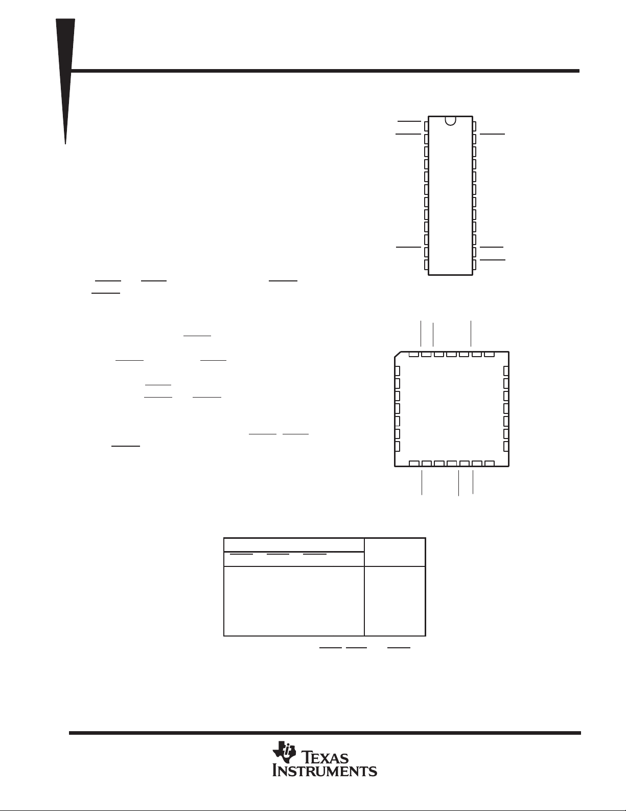
SN54BCT543 . . . JT OR W PACKAGE
SN74BCT543 . . . DW OR NT PACKAGE
LEBA
OEBA
CEAB
GND
SN54BCT543 . . . FK PACKAGE
A2
A3
A4
NC
A5
10
A6
A7
NC – No internal connection
†
OUTPUT
B
‡
0
, LEBA, and OEBA.
(TOP VIEW)
NC
24
23
22
21
20
19
18
17
16
15
14
13
CC
V
OEAB
V
CC
CEBA
B1
B2
B3
B4
B5
B6
B7
B8
LEAB
OEAB
B1
25
24
23
22
21
20
19
B8
LEAB
B2
B3
B4
NC
B5
B6
B7
1
2
3
A1
4
A2
5
A3
6
A4
7
A5
8
A6
9
A7
10
A8
11
12
(TOP VIEW)
A1
OEBA
LEBANCCEBA
3212827
426
5
6
7
8
9
11
12 13
14 15 16 1718
A8
GND
CEAB
PRODUCTION DATA information is current as of publication date.
Products conform to specifications per the terms of Texas Instruments
standard warranty. Production processing does not necessarily include
testing of all parameters.
POST OFFICE BOX 655303 • DALLAS, TEXAS 75265
Copyright 1994, Texas Instruments Incorporated
2–1
SN54BCT543, SN74BCT543
OCTAL REGISTERED TRANSCEIVERS
WITH 3-STATE OUTPUTS
SCBS026C – NOVEMBER 1988 – REVISED APRIL 1994
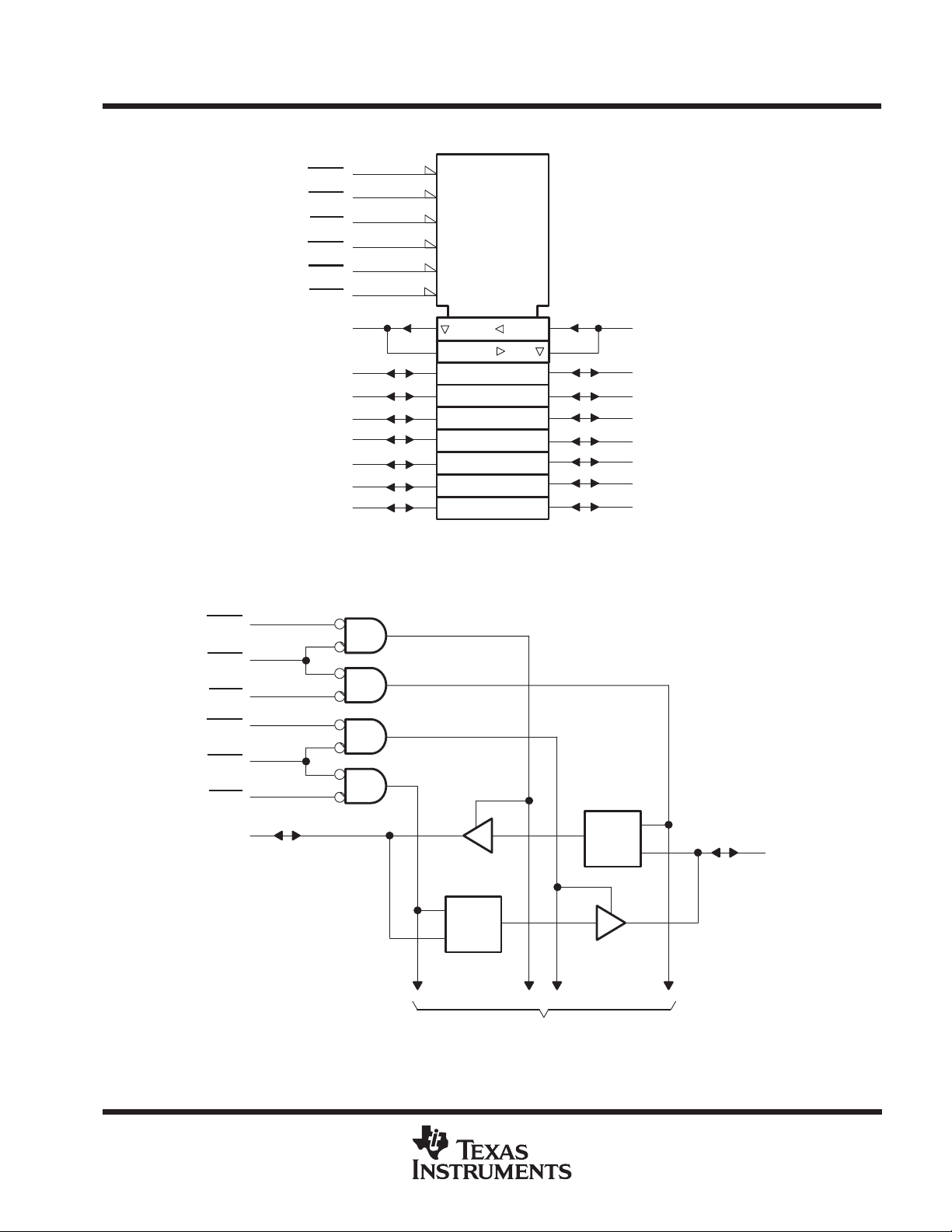
logic symbol
†
This symbol is in accordance with ANSI/IEEE Std 91-1984 and IEC Publication 617-12.
†
OEBA
CEBA
LEBA
OEAB
CEAB
LEAB
A1
A2
A3
A4
A5
A6
A7
A8
2
23
1
13
11
14
3
4
5
6
7
8
9
10
1EN3
G1
1C5
2EN4
G2
2C6
3
6D
5D
1
1
4
22
21
20
19
18
17
16
15
B1
B2
B3
B4
B5
B6
B7
B8
logic diagram (positive logic)
A1
2
23
1
13
11
14
3
OEBA
CEBA
LEBA
OEAB
CEAB
LEAB
C1
1D
C1
1D
22
B1
Pin numbers shown are for the DW, JT, NT, and W packages.
2–2
POST OFFICE BOX 655303 • DALLAS, TEXAS 75265
To Seven Other Channels
SN54BCT543, SN74BCT543
UNIT
OCTAL REGISTERED TRANSCEIVERS
WITH 3-STATE OUTPUTS
SCBS026C – NOVEMBER 1988 – REVISED APRIL 1994
absolute maximum ratings over operating free-air temperature range (unless otherwise noted)
Supply voltage range, V
CC
Input voltage range: Control inputs (see Note 1) – 0.5 V to 7 V. . . . . . . . . . . . . . . . . . . . . . . . . . . . . . . . . . . . . . . .
I/O ports (see Note 1) – 0.5 V to 5.5 V. . . . . . . . . . . . . . . . . . . . . . . . . . . . . . . . . . . . . . . . . .
Voltage range applied to any output in the disabled or power-off state, V
Voltage range applied to any output in the high state, V
Input clamp current, I
–30 mA. . . . . . . . . . . . . . . . . . . . . . . . . . . . . . . . . . . . . . . . . . . . . . . . . . . . . . . . . . . . . . . . . .
IK
. . . . . . . . . . . . . . . . . . . . . . . . . . . . . . .
O
O
Current into any output in the low state: SN54BCT543 96 mA. . . . . . . . . . . . . . . . . . . . . . . . . . . . . . . . . . . . . . . .
SN74BCT543 128 mA. . . . . . . . . . . . . . . . . . . . . . . . . . . . . . . . . . . . . . .
Operating free-air temperature range: SN54BCT543 – 55°C to 125°C. . . . . . . . . . . . . . . . . . . . . . . . . . . . . . . .
SN74BCT543 0°C to 70°C. . . . . . . . . . . . . . . . . . . . . . . . . . . . . . . . . . . .
Storage temperature range – 65°C to 150°C. . . . . . . . . . . . . . . . . . . . . . . . . . . . . . . . . . . . . . . . . . . . . . . . . . . . . . . .
†
Stresses beyond those listed under “absolute maximum ratings” may cause permanent damage to the device. These are stress ratings only, and
functional operation of the device at these or any other conditions beyond those indicated under “recommended operating conditions” is not
implied. Exposure to absolute-maximum-rated conditions for extended periods may affect device reliability.
NOTE 1: The input and output voltage ratings may be exceeded if the input and output current ratings are observed.
– 0.5 V to 7 V. . . . . . . . . . . . . . . . . . . . . . . . . . . . . . . . . . . . . . . . . . . . . . . . . . . . . . . . . .
– 0.5 V to 7 V. . . . . . . . . . . . . . . . .
– 0.5 V to V
recommended operating conditions
SN54BCT543 SN74BCT543
MIN NOM MAX MIN NOM MAX
V
V
V
I
I
I
T
CC
IH
IL
IK
OH
OL
A
Supply voltage 4.5 5 5.5 4.5 5 5.5 V
High-level input voltage 2 2 V
Low-level input voltage 0.8 0.8 V
Input clamp current –18 –18 mA
High-level output current –12 –15 mA
Low-level output current 48 64 mA
Operating free-air temperature –55 125 0 70 °C
†
CC
POST OFFICE BOX 655303 • DALLAS, TEXAS 75265
2–3

SN54BCT543, SN74BCT543
PARAMETER
TEST CONDITIONS
UNIT
VOLV
V
V
I
‡
V
5.5 V
V
2.7 V
A
I
‡
V
5.5 V
V
0.5 V
mA
OCTAL REGISTERED TRANSCEIVERS
WITH 3-STATE OUTPUTS
SCBS026C – NOVEMBER 1988 – REVISED APRIL 1994
electrical characteristics over recommended operating free-air temperature range (unless
otherwise noted)
SN54BCT543 SN74BCT543
MIN TYP†MAX MIN TYP†MAX
V
IK
V
OH
I
I
IH
IL
I
OS
I
CCL
I
CCH
I
CCZ
C
i
C
io
†
All typical values are at VCC = 5 V, TA = 25°C.
‡
For I/O ports, the parameters IIH and IIL include the off-state output current.
§
Not more than one output should be tested at a time, and the duration of the test should not exceed one second.
A or B port
Control input
A or B port
Control input
§
A or B port VCC = 5.5 V 45 71 45 71 mA
A or B port VCC = 5.5 V 5 8 5 8 mA
A or B port VCC = 5.5 V 9 15 9 15 mA
Control input VCC = 5 V, VI = 2.5 V or 0.5 V 6 6 pF
A or B port VCC = 5 V, VO = 2.5 V or 0.5 V 16 16 pF
VCC = 4.5 V, II = –18 mA –1.2 –1.2 V
IOH = –3 mA 2.4 3.3 2.4 3.3
VCC = 4.5 V
= 4.5
CC
VCC = 5.5 V, VI = 5.5 V 0.4 0.4 mA
,
=
CC
,
=
CC
VCC = 5.5 V, VO = 0 –100 –225 –100 –225 mA
IOH = –12 mA 2 3.2
IOH = –15 mA 2 3.1
IOL = 48 mA 0.38 0.55
IOL = 64 mA 0.42 0.55
=
I
=
I
70 70
20 20
–0.65 –0.65
–0.6 –0.6
V
µ
timing requirements over recommended ranges of supply voltage and operating free-air
temperature (unless otherwise noted)
VCC = 5 V,
TA = 25°C
MIN MAX MIN MAX MIN MAX
t
w
t
su
t
h
Pulse duration, LEAB or LEBA low 7 8 7 ns
Setup time, data before LEAB or LEBA↑ High or low 4.5 5.5 4.5 ns
Hold time, data after LEAB or LEBA↑ High or low 1.5 1.5 1.5 ns
SN54BCT543 SN74BCT543
UNIT
2–4
POST OFFICE BOX 655303 • DALLAS, TEXAS 75265

SN54BCT543, SN74BCT543
A or B
B or A
ns
LE
A or B
ns
OE
A or B
ns
OE
A or B
ns
CE
A or B
ns
CE
A or B
ns
OCTAL REGISTERED TRANSCEIVERS
WITH 3-STATE OUTPUTS
SCBS026C – NOVEMBER 1988 – REVISED APRIL 1994
switching characteristics (see Note 2)
VCC = 5 V,
CL = 50 pF,
PARAMETER
t
PLH
t
PHL
t
PLH
t
PHL
t
PZH
t
PZL
t
PHZ
t
PLZ
t
PZH
t
PZL
t
PHZ
t
†
NOTE 2: Load circuits and voltage waveforms are shown in Section 1.
PLZ
For conditions shown as MIN or MAX, use the appropriate value specified under recommended operating conditions.
FROM
(INPUT)
TO
(OUTPUT)
R1 = 500 Ω,
R2 = 500 Ω,
TA = 25°C
′BCT543 SN54BCT543 SN74BCT543
MIN TYP MAX MIN MAX MIN MAX
2 5.7 7.5 2 9.9 2 8.8
2 6.3 8.2 2 9.7 2 9.6
2 8.2 10.3 2 13.9 2 12.9
2 8.5 10.6 2 13.2 2 12.7
1 6.8 8.6 1 11.4 1 10.7
1 8.7 10.8 1 12.8 1 12.3
1 5.5 7.2 1 8.8 1 8.1
1 4.7 6.4 1 8.1 1 7.2
1 7.6 9.8 1 12.8 1 12
1 9.5 11.6 1 13.8 1 13.5
1 5.8 7.5 1 9.3 1 8.5
1 4.8 6.7 1 8.4 1 7.6
VCC = 4.5 V to 5.5 V,
CL = 50 pF,
R1 = 500 Ω,
R2 = 500 Ω,
TA = MIN to MAX
†
UNIT
POST OFFICE BOX 655303 • DALLAS, TEXAS 75265
2–5

SN54BCT543, SN74BCT543
OCTAL REGISTERED TRANSCEIVERS
WITH 3-STATE OUTPUTS
SCBS026C – NOVEMBER 1988 – REVISED APRIL 1994
2–6
POST OFFICE BOX 655303 • DALLAS, TEXAS 75265

IMPORTANT NOTICE
T exas Instruments and its subsidiaries (TI) reserve the right to make changes to their products or to discontinue
any product or service without notice, and advise customers to obtain the latest version of relevant information
to verify, before placing orders, that information being relied on is current and complete. All products are sold
subject to the terms and conditions of sale supplied at the time of order acknowledgement, including those
pertaining to warranty, patent infringement, and limitation of liability.
TI warrants performance of its semiconductor products to the specifications applicable at the time of sale in
accordance with TI’s standard warranty. Testing and other quality control techniques are utilized to the extent
TI deems necessary to support this warranty . Specific testing of all parameters of each device is not necessarily
performed, except those mandated by government requirements.
CERTAIN APPLICATIONS USING SEMICONDUCTOR PRODUCTS MAY INVOLVE POTENTIAL RISKS OF
DEATH, PERSONAL INJURY, OR SEVERE PROPERTY OR ENVIRONMENTAL DAMAGE (“CRITICAL
APPLICATIONS”). TI SEMICONDUCTOR PRODUCTS ARE NOT DESIGNED, AUTHORIZED, OR
WARRANTED TO BE SUITABLE FOR USE IN LIFE-SUPPORT DEVICES OR SYSTEMS OR OTHER
CRITICAL APPLICA TIONS. INCLUSION OF TI PRODUCTS IN SUCH APPLICATIONS IS UNDERST OOD TO
BE FULLY AT THE CUSTOMER’S RISK.
In order to minimize risks associated with the customer’s applications, adequate design and operating
safeguards must be provided by the customer to minimize inherent or procedural hazards.
TI assumes no liability for applications assistance or customer product design. TI does not warrant or represent
that any license, either express or implied, is granted under any patent right, copyright, mask work right, or other
intellectual property right of TI covering or relating to any combination, machine, or process in which such
semiconductor products or services might be or are used. TI’s publication of information regarding any third
party’s products or services does not constitute TI’s approval, warranty or endorsement thereof.
Copyright 1998, Texas Instruments Incorporated
 Loading...