

Texas Instruments SN74BCT373DBLE, SN74BCT373DBR, SN74BCT373DW, SN74BCT373DWR, SN74BCT373N Datasheet
...
SN54BCT373, SN74BCT373
OCTAL TRANSPARENT D-TYPE LATCHES
WITH 3-STATE OUTPUTS
SCBS016C – SEPTEMBER 1988 – REVISED NOVEMBER 1993
Copyright 1993, Texas Instruments Incorporated
2–1
POST OFFICE BOX 655303 • DALLAS, TEXAS 75265
• State-of-the-Art BiCMOS Design
Significantly Reduces Standby Current
• Full Parallel Access for Loading
• 3-State True Outputs Drive Bus Lines
or Buffer Memory Address Registers
• ESD Protection Exceeds 2000 V
Per MIL-Std-883C, Method 3015
• Package Options Include Plastic
Small-Outline (DW) and Shrink
Small-Outline (DB) Packages, Ceramic Chip
Carriers (FK) and Flatpacks (W), and
Standard Plastic and Ceramic 300-mil DIPs
(J, N)
description
These 8-bit latches feature 3-state outputs
designed specifically for driving highly capacitive
or relatively low-impedance loads. They are
particularly suitable for implementing buffer
registers, I/O ports, bidirectional bus drivers, and
working registers.
The eight latches of the ′BCT373 are transparent
D-type latches. While the latch-enable (LE) input
is high, the Q outputs will follow the data (D) inputs.
When the latch enable is taken low, the Q outputs
will be latched at the logic levels that were set up
at the D inputs.
A buffered output-enable (OE
) input can be used to place the eight outputs in either a normal logic state (high
or low logic levels) or a high-impedance state. In the high-impedance state, the outputs neither load nor drive
the bus lines significantly. The high-impedance state and increased drive provide the capability to drive bus
lines without need for interface or pullup components.
The output enable (OE) does not affect the internal operations of the latches. Old data can be retained or new
data can be entered while the outputs are in the high-impedance state.
The SN74BCT373 is available in TI’s shrink small-outline package (DB), which provides the same I/O pin count
and functionality of standard small-outline packages in less than half the printed-circuit-board area.
The SN54BCT373 is characterized for operation over the full military temperature range of –55°C to 125°C. The
SN74BCT373 is characterized for operation from 0°C to 70°C.
FUNCTION TABLE
(each latch)
INPUTS
OUTPUT
OE LE D
Q
L H H H
L HL L
L LX Q
0
H X X Z
1
2
3
4
5
6
7
8
9
10
20
19
18
17
16
15
14
13
12
11
OE
1Q
1D
2D
2Q
3Q
3D
4D
4Q
GND
V
CC
8Q
8D
7D
7Q
6Q
6D
5D
5Q
LE
SN54BCT373 ...J OR W PACKAGE
SN74BCT373 . . . DB, DW, OR N PACKAGE
(TOP VIEW)
3 2 1 20 19
910111213
4
5
6
7
8
18
17
16
15
14
8D
7D
7Q
6Q
6D
2D
2Q
3Q
3D
4D
1D1QOE
5Q
5D
8Q
4Q
GND
LE
V
CC
SN54BCT373 . . . FK PACKAGE
(TOP VIEW)
PRODUCTION DATA information is current as of publication date.
Products conform to specifications per the terms of Texas Instruments
standard warranty. Production processing does not necessarily include
testing of all parameters.
SN54BCT373, SN74BCT373
OCTAL TRANSPARENT D-TYPE LATCHES
WITH 3-STATE OUTPUTS
SCBS016C – SEPTEMBER 1988 – REVISED NOVEMBER 1993
2–2
POST OFFICE BOX 655303 • DALLAS, TEXAS 75265
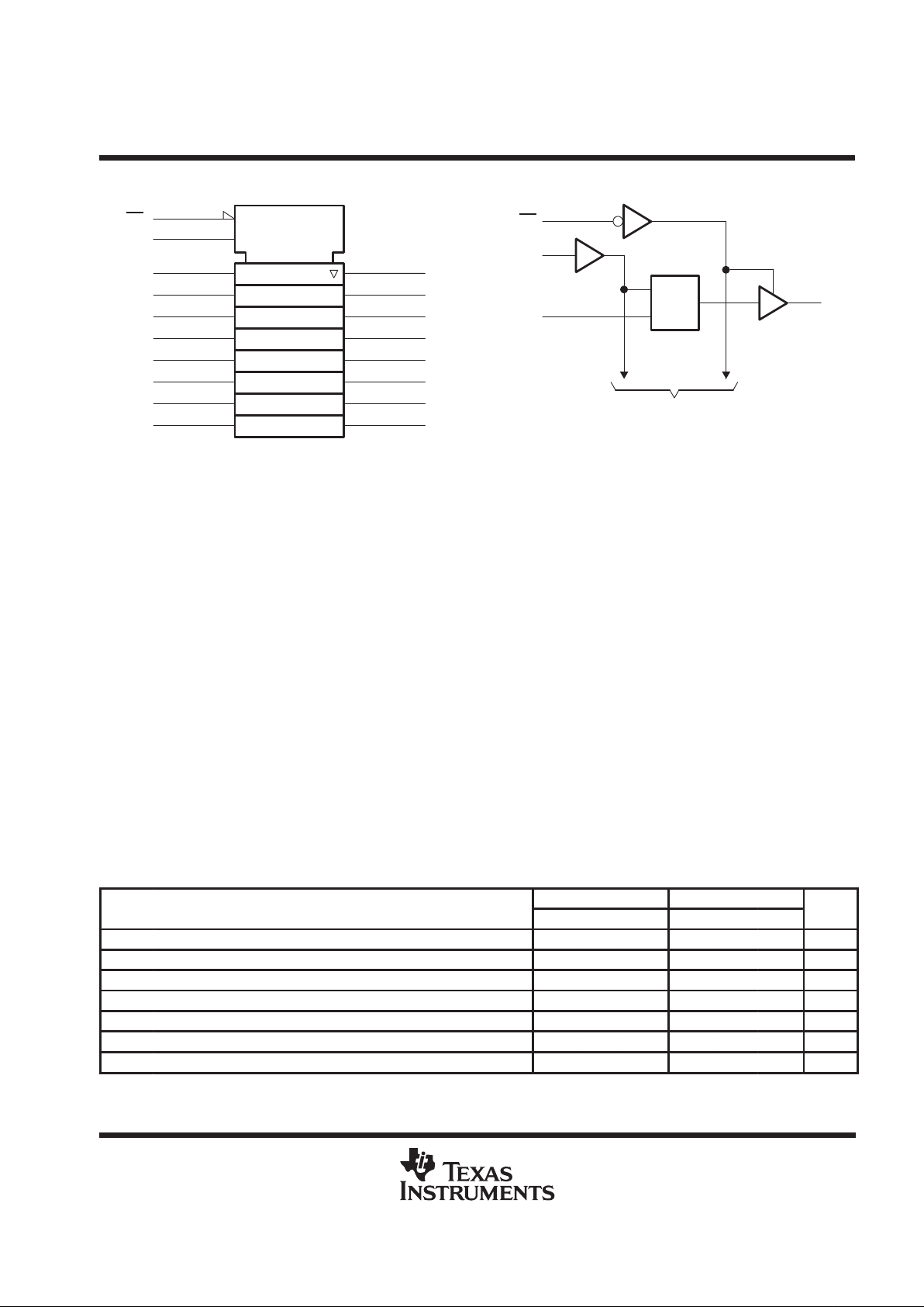
logic symbol
†
logic diagram (positive logic)
OE
1D
3
1D
4
2D
7
3D
8
4D
13
5D
C1
11
LE
1Q
2
2Q
5
3Q
6
4Q
9
5Q
12
6Q
15
7Q
16
8Q
19
14
6D
17
7D
18
8D
EN
1
OE
LE
1D
1Q
1
11
3
2
To Seven Other Channels
C1
1D
†
This symbol is in accordance with ANSI/IEEE Std 91-1984
and IEC Publication 617-12.
absolute maximum ratings over operating free-air temperature range (unless otherwise noted)
‡
Supply voltage range, V
CC
– 0.5 V to 7 V. . . . . . . . . . . . . . . . . . . . . . . . . . . . . . . . . . . . . . . . . . . . . . . . . . . . . . . . . .
Input voltage range, VI (see Note 1) – 0.5 V to 7 V. . . . . . . . . . . . . . . . . . . . . . . . . . . . . . . . . . . . . . . . . . . . . . . . . . .
Voltage range applied to any output in the disabled or power-off state, V
O
– 0.5 V to 5.5 V. . . . . . . . . . . . . . .
Voltage range applied to any output in the high state, V
O
– 0.5 V to V
CC
. . . . . . . . . . . . . . . . . . . . . . . . . . . . . . .
Input clamp current –30 mA. . . . . . . . . . . . . . . . . . . . . . . . . . . . . . . . . . . . . . . . . . . . . . . . . . . . . . . . . . . . . . . . . . . .
Current into any output in the low state: SN54BCT373 96 mA. . . . . . . . . . . . . . . . . . . . . . . . . . . . . . . . . . . . . . . .
SN74BCT373 128 mA. . . . . . . . . . . . . . . . . . . . . . . . . . . . . . . . . . . . . . .
Power dissipation (DB package only) (see Note 2) 650 mW. . . . . . . . . . . . . . . . . . . . . . . . . . . . . . . . . . . . . . . . . .
Operating free-air temperature range: SN54BCT373 – 55°C to 125°C. . . . . . . . . . . . . . . . . . . . . . . . . . . . . . . .
SN74BCT373 0°C to 70°C. . . . . . . . . . . . . . . . . . . . . . . . . . . . . . . . . . . .
Storage temperature range – 65°C to 150°C. . . . . . . . . . . . . . . . . . . . . . . . . . . . . . . . . . . . . . . . . . . . . . . . . . . . . . . .
‡
Stresses beyond those listed under “absolute maximum ratings” may cause permanent damage to the device. These are stress ratings only, and
functional operation of the device at these or any other conditions beyond those indicated under “recommended operating conditions” is not
implied. Exposure to absolute-maximum-rated conditions for extended periods may affect device reliability.
NOTES: 1. The input and output voltage ratings may be exceeded if the input and output current ratings are observed.
2. Power dissipation is application dependent and is a function of supply voltage, operating temperature, the number of outputs
switching simultaneously , and output duty cycle. Because the thermal resistance of the DB package is higher than that of the DW
or N packages, the DB package may not be suitable for some applications.
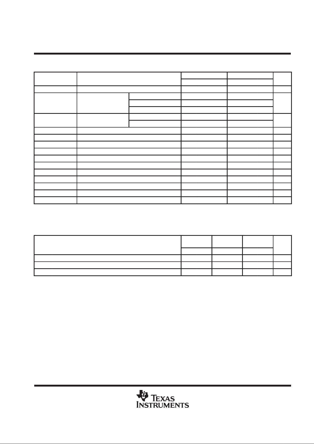
recommended operating conditions
SN54BCT373 SN74BCT373
MIN NOM MAX MIN NOM MAX
UNIT
V
CC
Supply voltage 4.5 5 5.5 4.5 5 5.5 V
V
IH
High-level input voltage 2 2 V
V
IL
Low-level input voltage 0.8 0.8 V
I
IK
Input clamp current –18 –18 mA
I
OH
High-level output current –12 –15 mA
I
OL
Low-level output current 48 64 mA
T
A
Operating free-air temperature –55 125 0 70 °C
SN54BCT373, SN74BCT373
OCTAL TRANSPARENT D-TYPE LATCHES
WITH 3-STATE OUTPUTS
SCBS016C – SEPTEMBER 1988 – REVISED NOVEMBER 1993
2–3
POST OFFICE BOX 655303 • DALLAS, TEXAS 75265
electrical characteristics over recommended operating free-air temperature range (unless
otherwise noted)
SN54BCT373 SN74BCT373
PARAMETER
TEST CONDITIONS
MIN TYP†MAX MIN TYP†MAX
UNIT
V
IK
VCC = 4.5 V, II = –18 mA –1.2 –1.2 V
IOH = –3 mA 2.4 3.3 2.4 3.3
V
OH
VCC = 4.5 V
IOH = –12 mA 2 3.2
V
IOH = –15 mA 2 3.1
IOL = 48 mA 0.38 0.55
V
OL
V
CC
= 4.5
V
IOL = 64 mA 0.42 0.55
V
I
I
VCC = 5.5 V, VI = 5.5 V 0.4 0.4 mA
I
IH
VCC = 5.5 V, VI = 2.7 V 20 20 µA
I
IL
VCC = 5.5 V, VI = 0.5 V –0.6 –0.6 mA
I
OS
‡
VCC = 5.5 V, VO = 0 –100 –225 –100 –225 mA
I
OZH
VCC = 5.5 V, VO = 2.7 V 50 50 µA
I
OZL
VCC = 5.5 V, VO = 0.5 V –50 –50 µA
I
CCL
VCC = 5.5 V 37 60 37 60 mA
I
CCH
VCC = 5.5 V 2 5 2 5 mA
I
CCZ
VCC = 5.5 V 5 8 5 8 mA
C
i
VCC = 5 V, VI = 2.5 V or 0.5 V 6 6 pF
C
o
VCC = 5 V, VO = 2.5 V or 0.5 V 11 11 pF
†
All typical values are at VCC = 5 V, TA = 25°C.
‡
Not more than one output should be tested at a time, and the duration of the test should not exceed one second.
timing requirements over recommended ranges of supply voltage and operating free-air
temperature (unless otherwise noted)
VCC = 5 V,
TA = 25°C
SN54BCT373 SN74BCT373
UNIT
MIN MAX MIN MAX MIN MAX
t
w
Pulse duration, LE high 7.5 7.5 7.5 ns
t
su
Setup time, data before LE↓ 2 2 2 ns
t
h
Hold time, data after LE↓ 5.5 5.5 5.5 ns
 Loading...