

SN54BCT29863B, SN74BCT29863B
9-BIT BUS TRANSCEIVERS
WITH 3-STATE OUTPUTS
SCBS015D – NOVEMBER 1988 – REVISED NOVEMBER 1993
Copyright 1993, Texas Instruments Incorporated
2–1
POST OFFICE BOX 655303 • DALLAS, TEXAS 75265
• BiCMOS Design Substantially Reduces I
CCZ
• Functionally Equivalent to ′ALS29863 and
AMD Am29863A
• Power-Up High-Impedance State
• ESD Protection Exceeds 2000 V Per
MIL-STD-883C, Method 3015
• Package Options Include Plastic
Small-Outline Packages (DW), Ceramic
Chip Carriers (FK) and Flatpacks (W), and
Standard Plastic and Ceramic 300-mil DIPs
(JT, NT)
description
These 9-bit transceivers are designed for
asynchronous communication between data
buses. The control-function implementation
allows for maximum flexibility in timing.
These devices allow data transmission from the A
bus to the B bus or from the B bus to the A bus,
depending upon the logic levels at the
output-enable (OEBA
and OEAB) inputs.
The outputs are in the high-impedance state
during power-up and power-down conditions. The
outputs remain in the high-impedance state while
the device is powered down.
The SN54BCT29863B is characterized for
operation over the full military temperature range
of –55°C to 125°C. The SN74BCT29863B is
characterized for operation from 0°C to 70°C.
FUNCTION TABLE
INPUTS
OEAB1 OEAB2 OEBA1 OEBA2
OPERATION
L L L L Latch A and B
L L H X
L LXH
A to B
H X L L
X HLL
B to A
H X H X
H XXH
X HXH
Isolation
X H H X
1
2
3
4
5
6
7
8
9
10
11
12
24
23
22
21
20
19
18
17
16
15
14
13
OEBA1
A1
A2
A3
A4
A5
A6
A7
A8
A9
OEBA2
GND
V
CC
B1
B2
B3
B4
B5
B6
B7
B8
B9
OEAB2
OEAB1
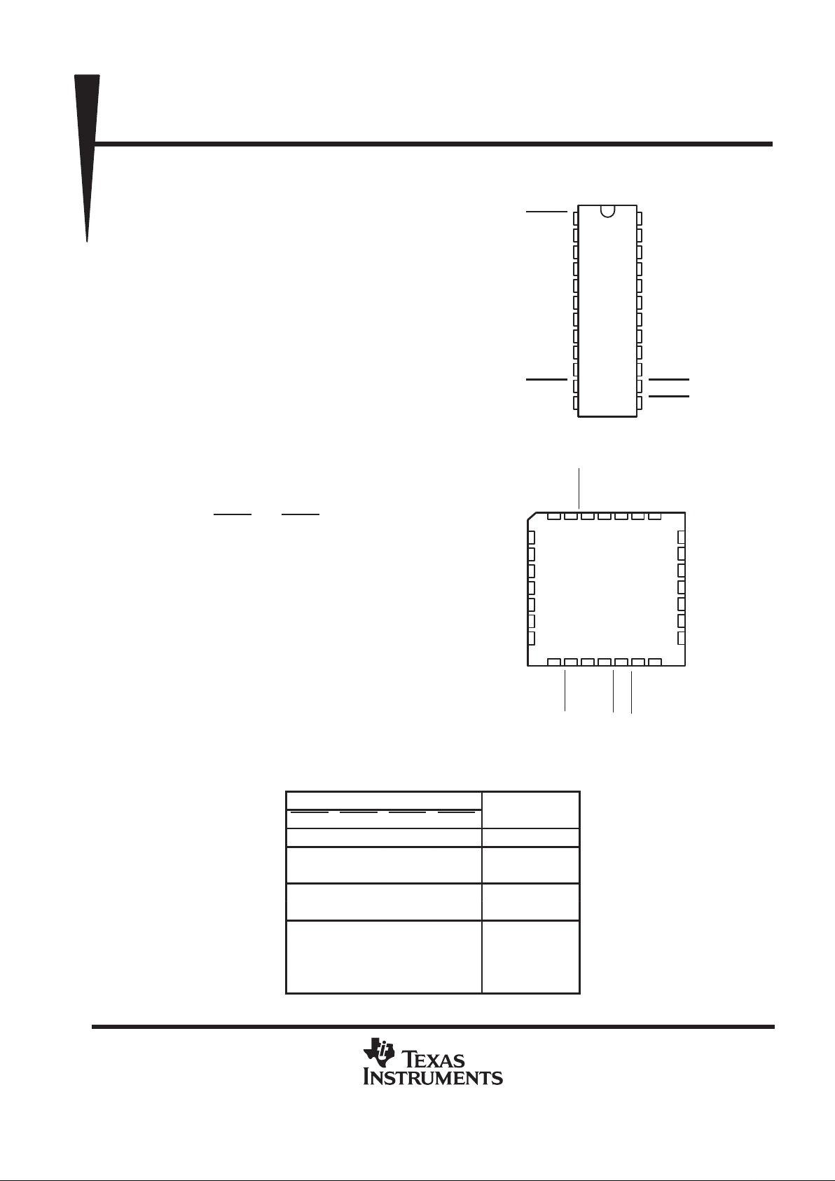
SN54BCT29863B . . . JT OR W PACKAGE
SN74BCT29863B . . . DW OR NT PACKAGE
(TOP VIEW)
321
13 14
5
6
7
8
9
10
11
B3
B4
B5
NC
B6
B7
B8
A3
A4
A5
NC
A6
A7
A8
4
15 16 17
18
GND
NC
OEAB1
B9
A2A1OEBA1
NC
SN54BCT29863B . . . FK PACKAGE
(TOP VIEW)
28 27 26
25
24
23
22
21
20
19
12
A9
B1
B2
V
CC
NC – No internal connection
OEBA2
OEAB2
PRODUCTION DATA information is current as of publication date.
Products conform to specifications per the terms of Texas Instruments
standard warranty. Production processing does not necessarily include
testing of all parameters.
SN54BCT29863B, SN74BCT29863B
9-BIT BUS TRANSCEIVERS
WITH 3-STATE OUTPUTS
SCBS015D – NOVEMBER 1988 – REVISED NOVEMBER 1993
2–2
POST OFFICE BOX 655303 • DALLAS, TEXAS 75265
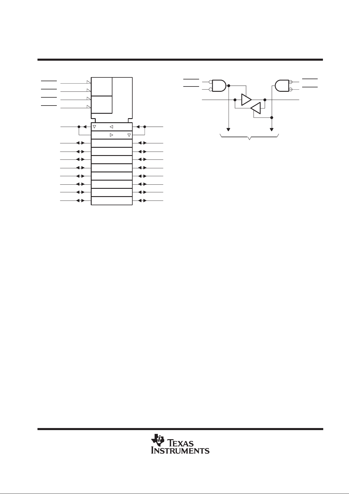
logic symbol
†
logic diagram (positive logic)
2
A1
1
11
13
14
B1
23
3
A2 B2
22
4
A3 B3
21
5
A4 B4
20
6
A5 B5
19
7
A6 B6
18
8
A7 B7
17
9
A8 B8
16
10
A9 B9
15
OEBA1
OEBA2
OEAB1
OEAB2
&
&
EN1
2
1
EN2
A1 B1
23
11
OEBA
1
1
2
14
13
OEBA2
OEAB1
OEAB2
To Eight Other Channels
†
This symbol is in accordance with ANSI/IEEE Std 91-1984
and IEC Publication 617-12.
Pin numbers shown are for the DW, JT, NT, and W packages.
absolute maximum ratings over operating free-air temperature range (unless otherwise noted)
‡
Supply voltage range, VCC –0.5 V to 7 V. . . . . . . . . . . . . . . . . . . . . . . . . . . . . . . . . . . . . . . . . . . . . . . . . . . . . . . . . .
Input voltage range (I/O ports) (see Note 1) –0.5 V to 5.5 V. . . . . . . . . . . . . . . . . . . . . . . . . . . . . . . . . . . . . . . . .
Input voltage range (excluding I/O ports) (see Note 1) –0.5 V to 7 V. . . . . . . . . . . . . . . . . . . . . . . . . . . . . . . . . .
Voltage range applied to any output in the high state –0.5 V to V
CC
. . . . . . . . . . . . . . . . . . . . . . . . . . . . . . . . . .
Input clamp current –30 mA. . . . . . . . . . . . . . . . . . . . . . . . . . . . . . . . . . . . . . . . . . . . . . . . . . . . . . . . . . . . . . . . . . . .
Current into any output in the low state: SN54BCT29863B 48 mA. . . . . . . . . . . . . . . . . . . . . . . . . . . . . . . . . . . .
SN74BCT29863B 96 mA. . . . . . . . . . . . . . . . . . . . . . . . . . . . . . . . . . . .
Operating free-air temperature range: SN54BCT29863B –55°C to 125°C. . . . . . . . . . . . . . . . . . . . . . . . . . . . .
SN74BCT29863B 0°C to 70°C. . . . . . . . . . . . . . . . . . . . . . . . . . . . . . . . .
Storage temperature range –65°C to 150°C. . . . . . . . . . . . . . . . . . . . . . . . . . . . . . . . . . . . . . . . . . . . . . . . . . . . . . .
‡
Stresses beyond those listed under “absolute maximum ratings” may cause permanent damage to the device. These are stress ratings only, and
functional operation of the device at these or any other conditions beyond those indicated under “recommended operating conditions” is not
implied. Exposure to absolute-maximum-rated conditions for extended periods may affect device reliability.
NOTE 1: The negative input voltage ratings may be exceeded if the input current rating is observed.
 Loading...