

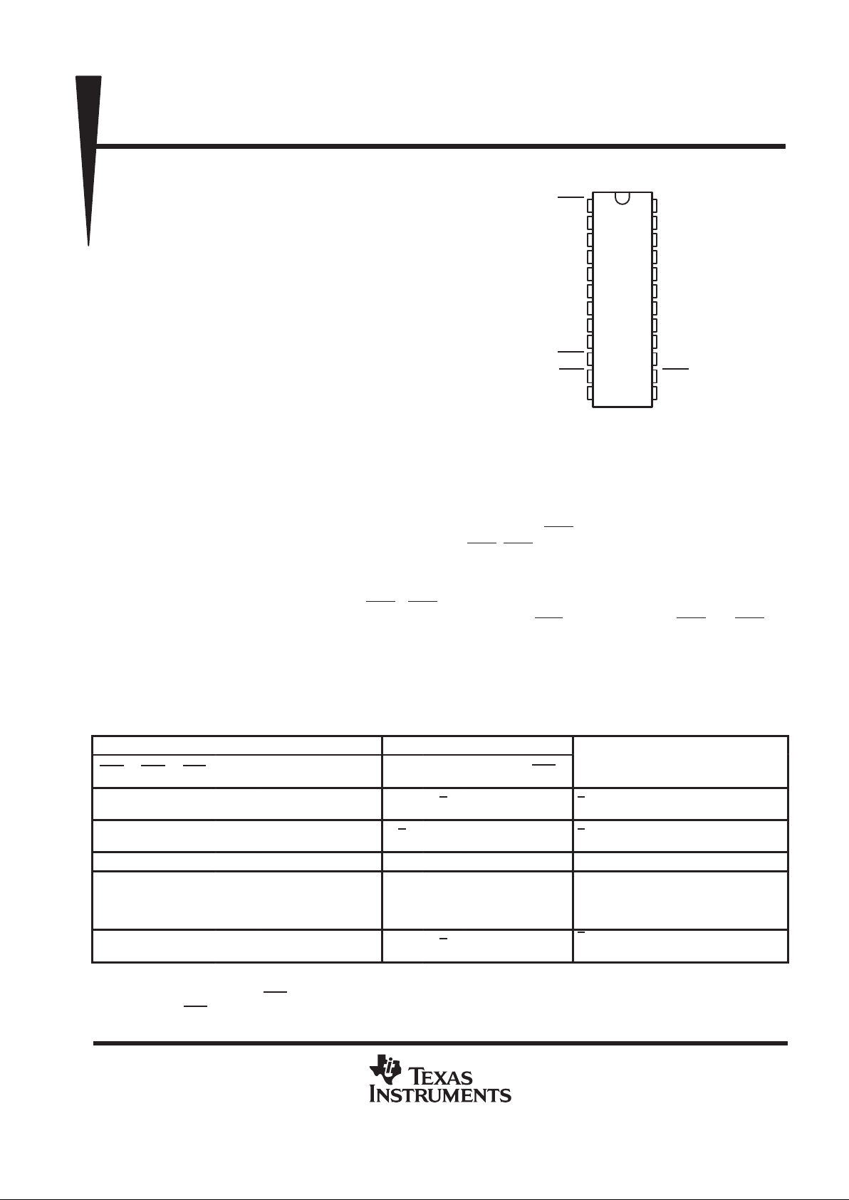
DW OR NT PACKAGE
(TOP VIEW)
1
2
3
4
5
6
7
8
9
10
11
12
24
23
22
21
20
19
18
17
16
15
14
13
OEA
A1
A2
A3
A4
A5
A6
A7
A8
ERR
CLR
GND
V
CC
B1
B2
B3
B4
B5
B6
B7
B8
PARITY
OEB
CLK
SN74BCT29834
8-BIT TO 9-BIT PARITY BUS TRANSCEIVER
SCBS256 – SEPTEMBER 1987 – REVISED NOVEMBER 1993
Copyright 1993, Texas Instruments Incorporated
2–1
POST OFFICE BOX 655303 • DALLAS, TEXAS 75265
• BiCMOS Process With TTL Inputs and
Outputs
• BiCMOS Design Reduces Standby Current
• Flow-Through Pinout (All Inputs on
Opposite Side From Outputs)
• Functionally Equivalent to SN74ALS29834
and AMD Am29834
• High-Speed Bus Transceiver With Parity
Generator/Checker
• Parity-Error Flag With Open-Collector
Output
• Available Register For Storage of the
Parity-Error Flag
• Package Options Include Plastic
Small-Outline (DW) Packages and Standard
Plastic 300-mil DIPs (NT)
description
The SN74BCT29834 is an 8-bit to 9-bit parity transceiver designed for asynchronous communication between
data buses. When data is transmitted from the A to B bus, a parity bit is generated. When data is transmitted
from the B to A bus with its corresponding parity bit, the parity-error (ERR) output will indicate whether or not
an error in the B data has occurred. The output-enable (OEA
, OEB) inputs can be used to disable the device
so that the buses are effectively isolated.
A 9-bit parity generator/checker generates a parity-odd (PARITY) output and monitors the parity of the I/O ports
with an open-collector parity-error flag (ERR). ERR is clocked into the register on the rising edge of the CLK
input. The error flag register is cleared with a low pulse on the clear (CLR) input. When both OEA and OEB are
low, data is transferred from the A bus to the B bus and inverted parity is generated. Inverted parity is a forced
error condition which gives the designer more system diagnostic capability. The SN74BCT29834 provides
inverting logic.
The SN74BCT29834 is characterized for operation from 0°C to 70°C.
FUNCTION TABLE
INPUTS
OUTPUT AND I/O
OEB OEA CLR
CLK
Ai
∑ of H’s
Bi
†
∑ of L’s
A B PARITY ERR
‡
FUNCTION
L H X X
Odd
Even
NA NA A
H
L
NA A data to B bus and generate parity
H L H ↑ NA
Odd
Even
B NA NA
H
L
B data to A bus and check parity
X X L X X X X NA NA H Clear error-flag register
H H
H
L
H
H
No↑
No↑
↑
↑
X
X
Odd
Even
X Z Z Z
NC
H
L
H
Isolation
§
L L X X
Odd
Even
NA NA A
L
H
NA
A data to B bus and generate inverted
parity
NA = not applicable, NC = no change, X = don’t care
†
Summation of high-level inputs includes PARITY along with Bi inputs.
‡
Output states shown assume the ERR
output was previously high.
§
In this mode, the ERR
output, when enabled, shows inverted parity of the A bus.
PRODUCTION DATA information is current as of publication date.
Products conform to specifications per the terms of Texas Instruments
standard warranty. Production processing does not necessarily include
testing of all parameters.
SN74BCT29834
8-BIT TO 9-BIT PARITY BUS TRANSCEIVER
SCBS256 – SEPTEMBER 1987 – REVISED NOVEMBER 1993
2–2
POST OFFICE BOX 655303 • DALLAS, TEXAS 75265
functional logic diagram (positive logic)
8x
EN
A1–A8
OEA
OEB
CLK
CLR
G1
1
1
1
1
MUX
2k
EN
8x
B1–B8
PARITY
ERR
88
8
8
8
9
P
R
C1
1D
SN74BCT29834
8-BIT TO 9-BIT PARITY BUS TRANSCEIVER
SCBS256 – SEPTEMBER 1987 – REVISED NOVEMBER 1993
2–3
POST OFFICE BOX 655303 • DALLAS, TEXAS 75265
error-flag waveforms
ERR
CLR
CLK
Bi + PARITY
OEA
OEB
Even
H
Odd
L
H
L
H
L
H
L
H
L
t
su
t
PLH
t
w
t
w
t
h
t
su
t
PHL
ERROR-FLAG FUNCTION TABLE
INPUTS
INTERNAL
TO DEVICE
OUTPUT
PRESTATE
OUTPUT
FUNCTION
CLR CLK
POINT P
ERR
n–1
†
ERR
FUNCTION
H
H
H
↑
↑
↑
H
X
L
H
L
X
H
L
L
Sample
L X X X H Clear
†
ERR
n–1
represents the state of the ERR output before any changes at CLR, CLK,
or point P.
absolute maximum ratings over operating free-air temperature range (unless otherwise noted)
‡
Supply voltage, V
CC
7 V. . . . . . . . . . . . . . . . . . . . . . . . . . . . . . . . . . . . . . . . . . . . . . . . . . . . . . . . . . . . . . . . . . . . . . . . .
Input voltage, V
I
7 V. . . . . . . . . . . . . . . . . . . . . . . . . . . . . . . . . . . . . . . . . . . . . . . . . . . . . . . . . . . . . . . . . . . . . . . . . . . . .
Voltage applied to a disabled I/O port 5.5 V. . . . . . . . . . . . . . . . . . . . . . . . . . . . . . . . . . . . . . . . . . . . . . . . . . . . . . . .
Operating free-air temperature range 0°C to 70°C. . . . . . . . . . . . . . . . . . . . . . . . . . . . . . . . . . . . . . . . . . . . . . . . . . .
Storage temperature range –65°C to 150°C. . . . . . . . . . . . . . . . . . . . . . . . . . . . . . . . . . . . . . . . . . . . . . . . . . . . . . . .
‡
Stresses beyond those listed under “absolute maximum ratings” may cause permanent damage to the device. These are stress ratings only, and
functional operation of the device at these or any other conditions beyond those indicated under “recommended operating conditions” is not
implied. Exposure to absolute-maximum-rated conditions for extended periods may affect device reliability.

SN74BCT29834
8-BIT TO 9-BIT PARITY BUS TRANSCEIVER
SCBS256 – SEPTEMBER 1987 – REVISED NOVEMBER 1993
2–4
POST OFFICE BOX 655303 • DALLAS, TEXAS 75265
recommended operating conditions
MIN NOM MAX UNIT
V
CC
Supply voltage 4.5 5 5.5 V
V
IH
High-level input voltage 2 V
V
IL
Low-level input voltage 0.8 V
V
OH
High-level output voltage, ERR 2.4 V
I
OH
High-level output current –24 mA
I
OL
Low-level output current 48 mA
T
A
Operating free-air temperature 0 70 °C
electrical characteristics over recommended operating free-air temperature range (unless
otherwise noted)
PARAMETER TEST CONDITIONS MIN TYP†MAX UNIT
V
IK
VCC = 4.5 V, II = –18 mA –1.2 V
IOH = –15 mA 2.4
V
OH
All i
nputs/outputs except
ERR
V
CC
= 4.5
V
IOH = –24 mA 2
V
I
OH
ERR VCC = 4.5 V, VOH = 2.4 V 20 µA
V
OL
VCC = 4.5 V, IOL = 48 mA 0.35 0.5 V
I
I
VCC = 5.5 V, VI = 5.5 V 0.1 mA
I
IH
‡
VCC = 5.5 V, VI = 2.7 V 20 µA
Data
–0.2
I
IL
‡
Control
V
CC
=
5.5 V
,
V
I
=
0.4 V
–0.75
mA
I
OS
§
VCC = 5.5 V, VO = 0 –75 –250 mA
I
CCL
VCC = 5.5 V, Outputs open 55 80 mA
I
CCZ
VCC = 5.5 V, Outputs open 30 45 mA
†
All typical values are at VCC = 5 V, TA = 25°C.
‡
These parameters include off-state output current for I/O ports only.
§
Not more than one output should be tested at a time, and the duration of the test should not exceed one second.
timing requirements over recommended ranges of supply voltage and operating free-air
temperature (unless otherwise noted)
MIN MAX UNIT
CLK high 10
t
w
Pulse duration
CLK low
10
ns
CLR low 10
Bi and PARITY 12
t
su
Set
up time before
CLK↑
CLR inactive 12
ns
t
h
Hold time after CLK↑
Bi and PARITY 0 ns

SN74BCT29834
8-BIT TO 9-BIT PARITY BUS TRANSCEIVER
SCBS256 – SEPTEMBER 1987 – REVISED NOVEMBER 1993
2–5
POST OFFICE BOX 655303 • DALLAS, TEXAS 75265
switching characteristics over recommended ranges of supply voltage and operating free-air
temperature, C
L
= 50 pF (unless otherwise noted) (see Note 1)
PARAMETER
FROM
(INPUT)
TO
(OUTPUT)
VCC = 5 V,
CL = 50 pF,
R1 = 500 Ω,
R2 = 500 Ω,
TA = 25°C
VCC = 4.5 V to 5.5 V,
CL = 50 pF,
R1 = 500 Ω,
R2 = 500 Ω,
TA = MIN to MAX
†
UNIT
MIN TYP MAX MIN MAX
t
PLH
1 5 7 1 8
t
PHL
A or B
B or A
1.5 4 6 1.5 7
ns
t
PLH
1.5 10 13 1.5 15
t
PHL
A
PARITY
1.5 8 10 1.5 15
ns
t
PZH
2 11 15 2 19
t
PZL
OEA
or
OEB
A or B
2 15 19 2 21
ns
t
PHZ
2 8 11 2 15
t
PLZ
OEA
or
OEB
A or B
2 13 17 2 21
ns
CLK
1.5 7 10 1.5 12
t
PLH
CLR
ERR
1.5 13 17 1.5 18
ns
t
PLH
1.5 10 13 1.5 15
t
PHL
OEA
PARITY
1.5 10 13 1.5 15
ns
†
For conditions shown as MIN or MAX, use the appropriate value specified under recommended operating conditions.
NOTE 1: Load circuits and voltage waveforms are shown in Section 1.

SN74BCT29834
8-BIT TO 9-BIT PARITY BUS TRANSCEIVER
SCBS256 – SEPTEMBER 1987 – REVISED NOVEMBER 1993
2–6
POST OFFICE BOX 655303 • DALLAS, TEXAS 75265

IMPORTANT NOTICE
T exas Instruments and its subsidiaries (TI) reserve the right to make changes to their products or to discontinue
any product or service without notice, and advise customers to obtain the latest version of relevant information
to verify, before placing orders, that information being relied on is current and complete. All products are sold
subject to the terms and conditions of sale supplied at the time of order acknowledgement, including those
pertaining to warranty, patent infringement, and limitation of liability.
TI warrants performance of its semiconductor products to the specifications applicable at the time of sale in
accordance with TI’s standard warranty. Testing and other quality control techniques are utilized to the extent
TI deems necessary to support this warranty. Specific testing of all parameters of each device is not necessarily
performed, except those mandated by government requirements.
CERT AIN APPLICATIONS USING SEMICONDUCTOR PRODUCTS MAY INVOLVE POTENTIAL RISKS OF
DEATH, PERSONAL INJURY, OR SEVERE PROPERTY OR ENVIRONMENTAL DAMAGE (“CRITICAL
APPLICATIONS”). TI SEMICONDUCTOR PRODUCTS ARE NOT DESIGNED, AUTHORIZED, OR
WARRANTED TO BE SUITABLE FOR USE IN LIFE-SUPPORT DEVICES OR SYSTEMS OR OTHER
CRITICAL APPLICATIONS. INCLUSION OF TI PRODUCTS IN SUCH APPLICA TIONS IS UNDERSTOOD T O
BE FULLY AT THE CUSTOMER’S RISK.
In order to minimize risks associated with the customer’s applications, adequate design and operating
safeguards must be provided by the customer to minimize inherent or procedural hazards.
TI assumes no liability for applications assistance or customer product design. TI does not warrant or represent
that any license, either express or implied, is granted under any patent right, copyright, mask work right, or other
intellectual property right of TI covering or relating to any combination, machine, or process in which such
semiconductor products or services might be or are used. TI’s publication of information regarding any third
party’s products or services does not constitute TI’s approval, warranty or endorsement thereof.
Copyright 1998, Texas Instruments Incorporated
 Loading...