

SN54BCT29827B, SN74BCT29827B
OUTPUT
10-BIT BUFFERS/DRIVERS
WITH 3-STATE OUTPUTS
SCBS008C – APRIL 1987 – REVISED NOVEMBER 1993
• State-of-the-Art BiCMOS Design
Significantly Reduces I
CCZ
• ESD Protection Exceeds 2000 V Per
MIL-STD-883C, Method 3015; Exceeds
200 V Using Machine Model (C = 200 pF,
R = 0)
• 3-State Outputs Drive Bus Lines or Buffer
Memory Address Registers
• P-N-P Inputs Reduce DC Loading
• Flow-Through Architecture Optimizes
PCB Layout
• Package Options Include Plastic
Small-Outline (DW) Packages, Ceramic Chip
Carriers (FK) and Flatpacks (W), and
Standard Plastic and Ceramic 300-mil DIPs
(JT, NT)
description
These 10-bit buffers and bus drivers provide
high-performance bus interface for wide data
paths or buses carrying parity.
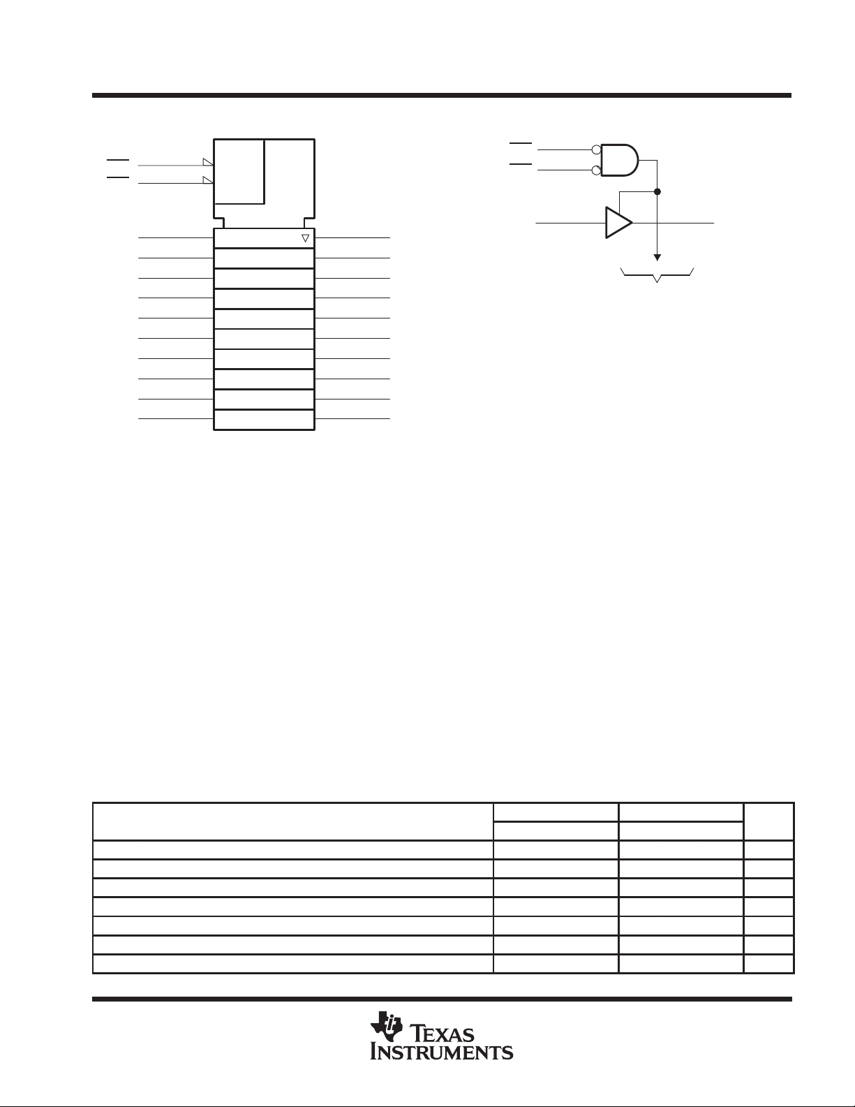
The 3-state control gate is a 2-input AND gate with
active-low inputs so that if either output-enable
(OE1
or OE2) input is high, all ten outputs are in
the high-impedance state. The outputs are also in
the high-impedance state during power-up and
power-down conditions. The outputs remain in the
high-impedance state while the device is powered
down.
The SN54BCT29827B is characterized for
operation over the full military temperature range
of –55°C to 125°C. The SN74BCT29827B is
characterized for operation from 0°C to 70°C.
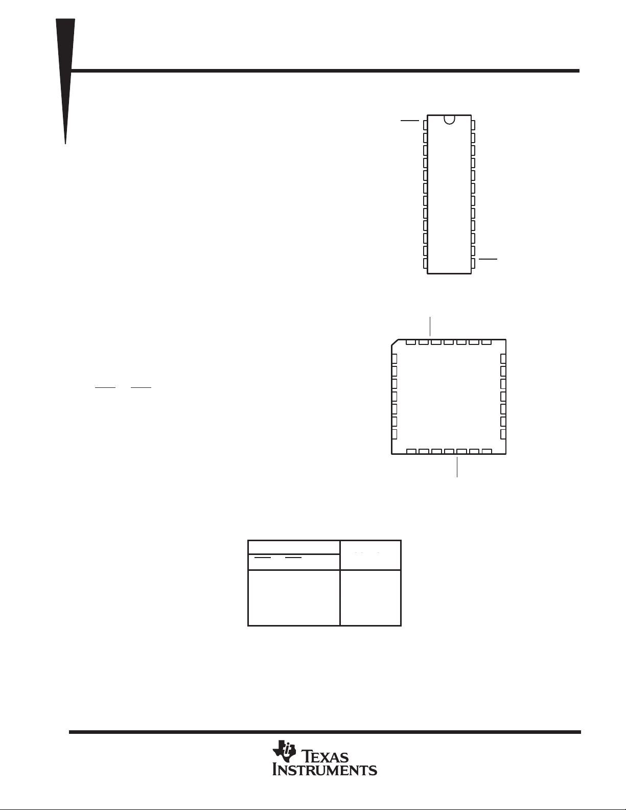
SN54BCT29827B . . . JT OR W PACKAGE
SN74BCT29827B . . . DW OR NT PACKAGE
SN54BCT29827B . . . FK PACKAGE
A3
A4
A5
NC
A6
A7
A8
NC – No internal connection
(TOP VIEW)
1
24
NC
23
22
21
20
19
18
17
16
15
14
13
CC
OE2
V
CC
Y1
Y2
Y3
Y4
Y5
Y6
Y7
Y8
Y9
Y10
OE2
Y1
Y10
Y2
25
24
23
22
21
20
19
Y9
Y3
Y4
Y5
NC
Y6
Y7
Y8
OE1
2
A1
3
A2
4
A3
5
A4
6
A5
7
A6
8
A7
9
A8
10
A9
11
A10
GND
12
(TOP VIEW)
A2A1OE1NCV
3 2 28 27
426
5
6
7
8
9
10
11
12 13
A9
1
14 15 16 17 18
A10
GND
PRODUCTION DATA information is current as of publication date.
Products conform to specifications per the terms of Texas Instruments
standard warranty. Production processing does not necessarily include
testing of all parameters.
FUNCTION TABLE
INPUTS
OE1 OE2 A
L L L L
L LH H
H XX Z
X H X Z
POST OFFICE BOX 655303 • DALLAS, TEXAS 75265
OUTPUT
Y
Copyright 1993, Texas Instruments Incorporated
2–1
SN54BCT29827B, SN74BCT29827B
UNIT
10-BIT BUFFERS/DRIVERS
WITH 3-STATE OUTPUTS
SCBS008C – APRIL 1987 – REVISED NOVEMBER 1993
1
13
2
3
4
5
6
7
8
9
10
11
†
&
EN
23
1
22
21
20
19
18
17
16
15
14
Y1
Y2
Y3
Y4
Y5
Y6
Y7
Y8
Y9
Y10
logic diagram (positive logic)
OE1
OE2
1
13
223
A1
To Nine Other Channels
Y1
logic symbol
OE1
OE2
A1
A2
A3
A4
A5
A6
A7
A8
A9
A10
†
This symbol is in accordance with ANSI/IEEE Std 91-1984
and IEC Publication 617-12.
Pin numbers shown are for the DW, JT, NT, and W packages.
absolute maximum ratings over operating free-air temperature range (unless otherwise noted)
‡
Supply voltage range, V
CC
–0.5 V to 7 V. . . . . . . . . . . . . . . . . . . . . . . . . . . . . . . . . . . . . . . . . . . . . . . . . . . . . . . . . .
Input voltage range, VI (see Note 1) –0.5 V to 7 V. . . . . . . . . . . . . . . . . . . . . . . . . . . . . . . . . . . . . . . . . . . . . . . . . . .
Voltage range applied to any output in the disabled or power-off state, V
Voltage range applied to any output in the high state, V
Input clamp current, I
(V
< 0) –30 mA. . . . . . . . . . . . . . . . . . . . . . . . . . . . . . . . . . . . . . . . . . . . . . . . . . . . . . . . . . . .
IK
I
. . . . . . . . . . . . . . . . . . . . . . . . . . . . . . .
O
O
–0.5 V to 5.5 V. . . . . . . . . . . . . . . .
–0.5 V to V
Current into any output in the low state, IO: SN54BCT29827B 48 mA. . . . . . . . . . . . . . . . . . . . . . . . . . . . . . . . .
SN74BCT29827B 96 mA. . . . . . . . . . . . . . . . . . . . . . . . . . . . . . . . .
Operating free-air temperature range: SN54BCT29827B –55°C to 125°C. . . . . . . . . . . . . . . . . . . . . . . . . . . . . .
SN74BCT29827B 0°C to 70°C. . . . . . . . . . . . . . . . . . . . . . . . . . . . . . . . . .
Storage temperature range –65°C to 150°C. . . . . . . . . . . . . . . . . . . . . . . . . . . . . . . . . . . . . . . . . . . . . . . . . . . . . . . .
‡
Stresses beyond those listed under “absolute maximum ratings” may cause permanent damage to the device. These are stress ratings only, and
functional operation of the device at these or any other conditions beyond those indicated under “recommended operating conditions” is not
implied. Exposure to absolute-maximum-rated conditions for extended periods may affect device reliability.
NOTE 1: The input and output negative-voltage ratings may be exceeded if the input and output clamp-current ratings are observed.
recommended operating conditions
SN54BCT29827B SN74BCT29827B
MIN NOM MAX MIN NOM MAX
V
V
V
I
I
I
T
CC
IH
IL
IK
OH
OL
A
Supply voltage 4.5 5 5.5 4.5 5 5.5 V
High-level input voltage 2 2 V
Low-level input voltage 0.8 0.8 V
Input clamp current –18 –18 mA
High-level output current –15 –24 mA
Low-level output current 24 48 mA
Operating free-air temperature –55 125 0 70 °C
CC
2–2
POST OFFICE BOX 655303 • DALLAS, TEXAS 75265
 Loading...