

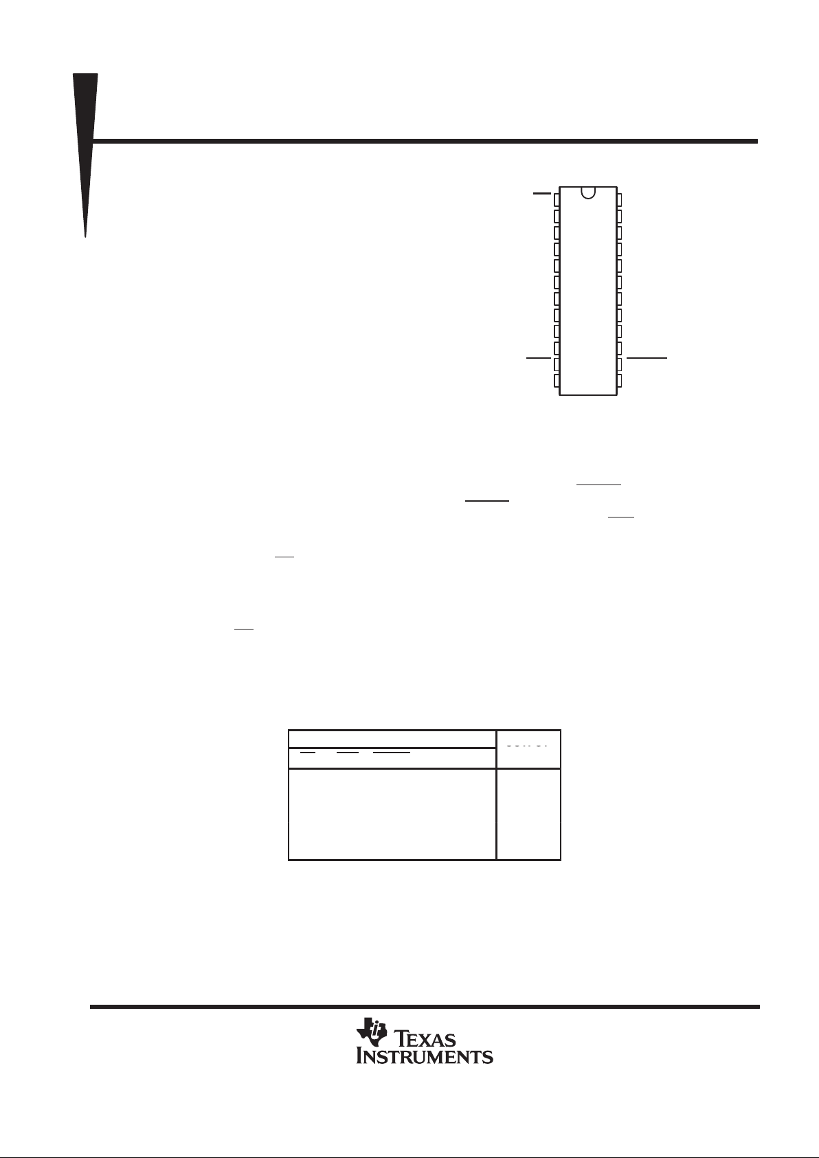
DW OR NT PACKAGE
(TOP VIEW)
1
2
3
4
5
6
7
8
9
10
11
12
24
23
22
21
20
19
18
17
16
15
14
13
OE
1D
2D
3D
4D
5D
6D
7D
8D
9D
CLR
GND
V
CC
1Q
2Q
3Q
4Q
5Q
6Q
7Q
8Q
9Q
CLKEN
CLK
SN74BCT29823
9-BIT BUS-INTERFACE FLIP-FLOP
WITH 3-STATE OUTPUTS
SCBS018D – NOVEMBER 1988 – REVISED NOVEMBER 1993
Copyright 1993, Texas Instruments Incorporated
2–1
POST OFFICE BOX 655303 • DALLAS, TEXAS 75265
• State-of-the-Art BiCMOS Design
Significantly Reduces I
CCZ
• ESD Protection Exceeds 2000 V Per
MIL-STD-883C, Method 3015; Exceeds
200 V Using Machine Model (C = 200 pF,
R = 0)
• 3-State Buffer-Type Outputs Drive Bus
Lines Directly
• Package Options Include Plastic
Small-Outline (DW) Packages and Standard
Plastic 300-mil DIPs (NT)
description
This 9-bit bus-interface flip-flop features 3-state
outputs designed specifically for driving highly
capacitive or relatively low-impedance loads. It is
particularly suitable for implementing wider buffer
registers, I/O ports, bidirectional bus drivers with
parity, and working registers.
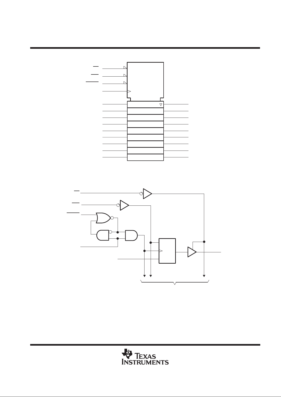
The nine flip-flops are edge-triggered D-type flip-flops. With the clock-enable (CLKEN
) input low, the flip-flops
store data on the low-to-high transitions of the clock. T aking CLKEN high disables the clock buf fer, thus latching
the outputs. The SN74BCT29823 has noninverting data (D) inputs. T aking the clear (CLR) input low causes the
nine Q outputs to go low independent of the clock.
A buffered output-enable (OE) input can be used to place the nine outputs in either a normal logic state (high
or low) or a high-impedance state. In the high-impedance state, the outputs neither load nor drive the bus lines
significantly . The high-impedance state and increased drive provide the capability to drive bus lines without need
for interface or pullup components.
The output enable (OE) does not affect the internal operation of the flip-flops. Old data can be retained or new
data can be entered while the outputs are in the high-impedance state.
The SN74BCT29823 is characterized for operation from 0°C to 70°C.
FUNCTION TABLE
(each flip-flop)
INPUTS
OUTPUT
OE CLR CLKEN CLK D
OUTPUT
Q
L L X X X L
L HL↑ HH
L HL↑ LL
L HHXX Q
0
H X X X X Z
PRODUCTION DATA information is current as of publication date.
Products conform to specifications per the terms of Texas Instruments
standard warranty. Production processing does not necessarily include
testing of all parameters.
SN74BCT29823
9-BIT BUS-INTERFACE FLIP-FLOP
WITH 3-STATE OUTPUTS
SCBS018D – NOVEMBER 1988 – REVISED NOVEMBER 1993
2–2
POST OFFICE BOX 655303 • DALLAS, TEXAS 75265
logic symbol
†
EN
1
7
6D
8
7D
9
8D
10
9D
2D
2
1D
6Q
18
7Q
17
8Q
16
9Q
15
1Q
23
3
2D
4
3D
5
4D
6
5D
2Q
22
3Q
21
4Q
20
5Q
19
OE
13
CLK 1C2
R
11
CLR
G1
14
CLKEN
†
This symbol is in accordance with ANSI/IEEE Std 91-1984 and IEC Publication 617-12.
logic diagram (positive logic)
To Eight Other Channels
23
2
1
1D
1Q
R
C1
1D
CLKEN
CLK
11
14
13
OE
CLR
 Loading...