

Texas Instruments SN74BCT29821DW, SN74BCT29821DWR, SN74BCT29821NT Datasheet
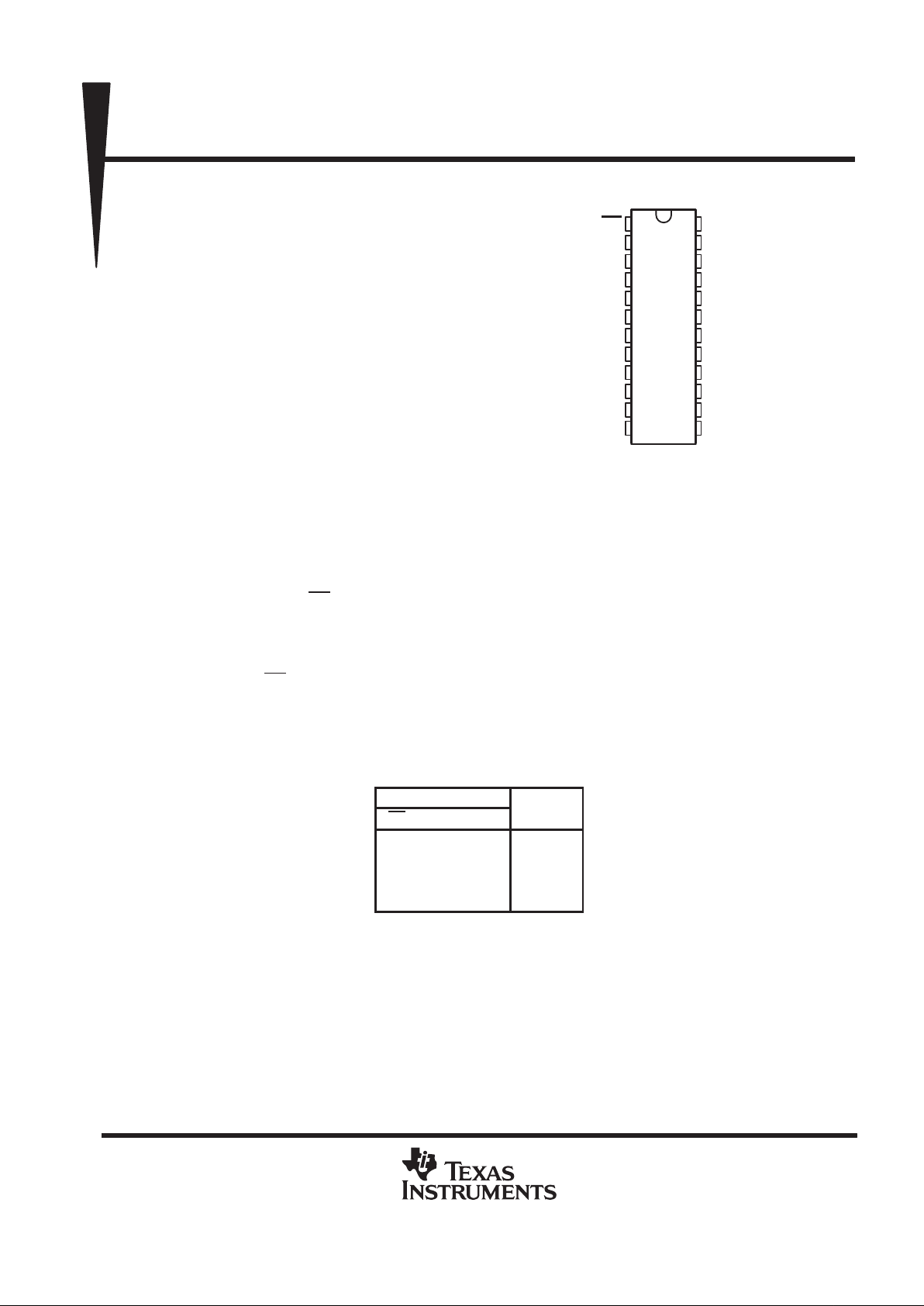
DW OR NT PACKAGE
(TOP VIEW)
1
2
3
4
5
6
7
8
9
10
11
12
24
23
22
21
20
19
18
17
16
15
14
13
OE
1D
2D
3D
4D
5D
6D
7D
8D
9D
10D
GND
V
CC
1Q
2Q
3Q
4Q
5Q
6Q
7Q
8Q
9Q
10Q
CLK
SN74BCT29821
10-BIT BUS-INTERFACE FLIP-FLOP
WITH 3-STATE OUTPUTS
SCBS021D – FEBRUARY 1989 – REVISED NOVEMBER 1993
Copyright 1993, Texas Instruments Incorporated
2–1
POST OFFICE BOX 655303 • DALLAS, TEXAS 75265
• State-of-the-Art BiCMOS Design
Significantly Reduces I
CCZ
• ESD Protection Exceeds 2000 V Per
MIL-STD-883C, Method 3015; Exceeds
200 V Using Machine Model (C = 200 pF,
R = 0)
• 3-State Buffer-Type Outputs Drive Bus
Lines Directly
• Package Options Include Plastic
Small-Outline (DW) Packages and Standard
Plastic 300-mil DIPs (NT)
description
This 10-bit bus-interface flip-flop features 3-state
outputs designed specifically for driving highly
capacitive or relatively low-impedance loads. It is
particularly suitable for implementing wider buffer
registers, I/O ports, bidirectional bus drivers with
parity, and working registers.
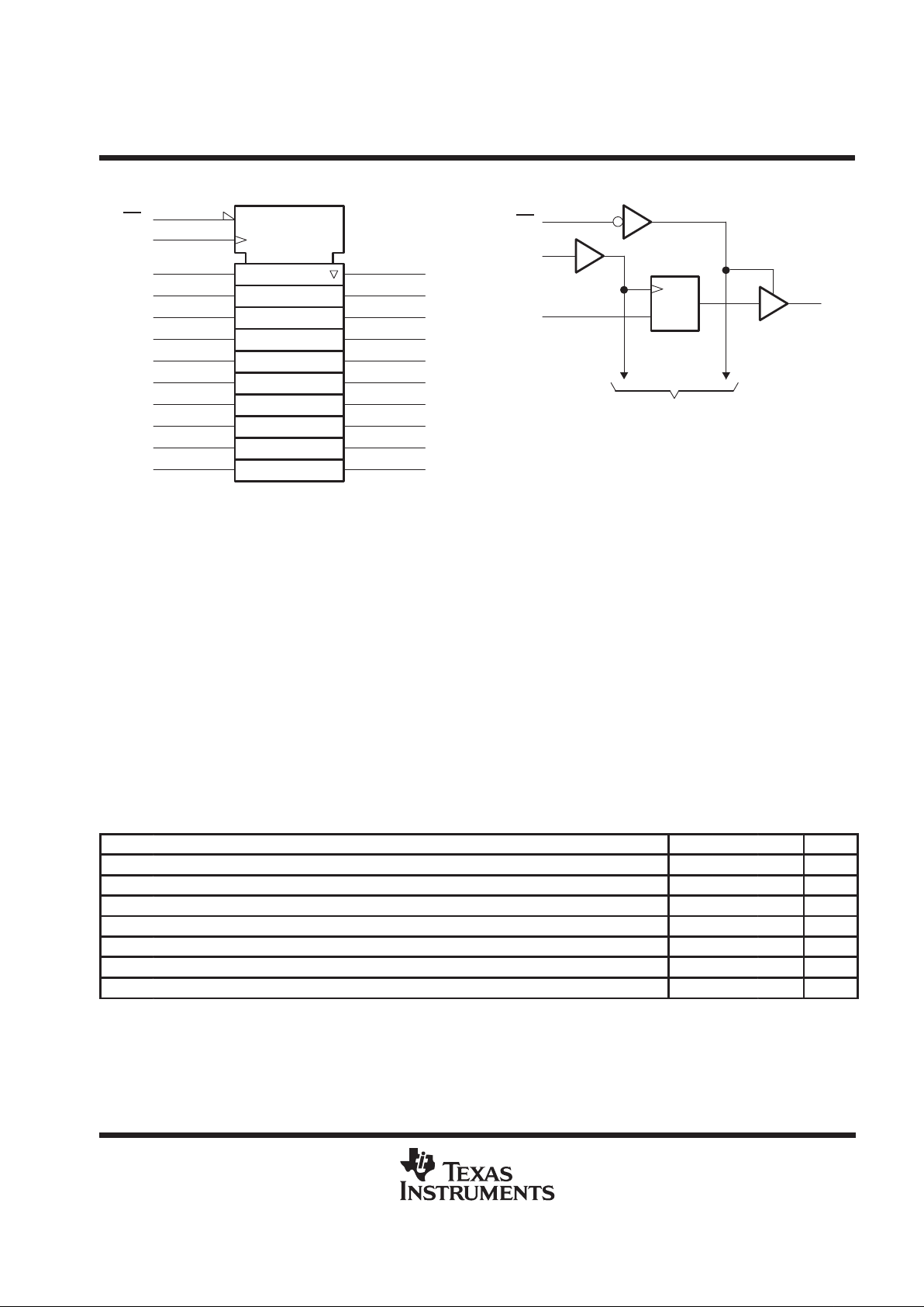
The ten flip-flops are edge-triggered D-type flip-flops. On the positive transition of the clock, the Q outputs will
be true to the data (D) inputs.
A buffered output-enable (OE) input can be used to place the ten outputs in either a normal logic state (high or
low) or a high-impedance state. In the high-impedance state, the outputs neither load nor drive the bus lines
significantly . The high-impedance state and increased drive provide the capability to drive bus lines without need
for interface or pullup components.
The output enable (OE
) does not affect the internal operation of the flip-flops. Old data can be retained or new
data can be entered while the outputs are in the high-impedance state.
The SN74BCT29821 is characterized for operation from 0°C to 70°C.
FUNCTION TABLE
(each flip-flop)
INPUTS
OUTPUT
OE CLK D
Q
L ↑ H H
L ↑ LL
L H or L X Q
0
H X X Z
PRODUCTION DATA information is current as of publication date.
Products conform to specifications per the terms of Texas Instruments
standard warranty. Production processing does not necessarily include
testing of all parameters.
SN74BCT29821
10-BIT BUS-INTERFACE FLIP-FLOP
WITH 3-STATE OUTPUTS
SCBS021D – FEBRUARY 1989 – REVISED NOVEMBER 1993
2–2
POST OFFICE BOX 655303 • DALLAS, TEXAS 75265
logic symbol
†
logic diagram (positive logic)
OE
1D
2
1D
3
2D
4
3D
5
4D
6
5D
13
CLK
C1
1Q
23
2Q
22
3Q
21
4Q
20
5Q
19
6Q
18
7Q
17
8Q
16
9Q
15
10Q
14
7
6D
8
7D
9
8D
10
9D
11
10D
EN
1
OE
CLK
1D
1Q
1
13
2
23
To Nine Other Channels
C1
1D
†
This symbol is in accordance with ANSI/IEEE Std 91-1984
and IEC Publication 617-12.
absolute maximum ratings over operating free-air temperature range (unless otherwise noted)
‡
Supply voltage range, V
CC
–0.5 V to 7 V. . . . . . . . . . . . . . . . . . . . . . . . . . . . . . . . . . . . . . . . . . . . . . . . . . . . . . . . . .
Input voltage range, VI (see Note 1) –0.5 V to 7 V. . . . . . . . . . . . . . . . . . . . . . . . . . . . . . . . . . . . . . . . . . . . . . . . . . .
Voltage range applied to any output in the disabled or power-off state, V
O
–0.5 V to 5.5 V. . . . . . . . . . . . . . . .
Voltage range applied to any output in the high state, V
O
–0.5 V to V
CC
. . . . . . . . . . . . . . . . . . . . . . . . . . . . . . .
Input clamp current, I
IK
(V
I
< 0) –30 mA. . . . . . . . . . . . . . . . . . . . . . . . . . . . . . . . . . . . . . . . . . . . . . . . . . . . . . . . . . . .
Current into any output in the low state, I
O
96 mA. . . . . . . . . . . . . . . . . . . . . . . . . . . . . . . . . . . . . . . . . . . . . . . . . . .
Operating free-air temperature range 0°C to 70°C. . . . . . . . . . . . . . . . . . . . . . . . . . . . . . . . . . . . . . . . . . . . . . . . . . .
Storage temperature range –65°C to 150°C. . . . . . . . . . . . . . . . . . . . . . . . . . . . . . . . . . . . . . . . . . . . . . . . . . . . . . . .
‡
Stresses beyond those listed under “absolute maximum ratings” may cause permanent damage to the device. These are stress ratings only, and
functional operation of the device at these or any other conditions beyond those indicated under “recommended operating conditions” is not
implied. Exposure to absolute-maximum-rated conditions for extended periods may affect device reliability.
NOTE 1: The input and output negative-voltage ratings may be exceeded if the input and output clamp-current ratings are observed.
recommended operating conditions
MIN NOM MAX UNIT
V
CC
Supply voltage 4.5 5 5.5 V
V
IH
High-level input voltage 2 V
V
IL
Low-level input voltage 0.8 V
I
IK
Input clamp current –18 mA
I
OH
High-level output current –24 mA
I
OL
Low-level output current 48 mA
T
A
Operating free-air temperature 0 70 °C
 Loading...