

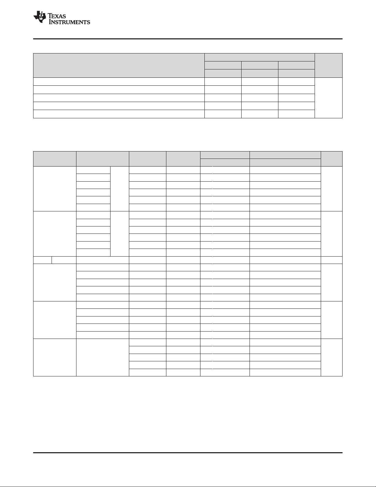
B1
DIR
5
7
A1
2
V
CCA
V
CCB
B2
6
A2
3
1
8
VCCA
VCCB
GND
4
V
CCA
V
CCB
Product
Folder
Sample &
Buy
Technical
Documents
Tools &
Software
Support &
Community
SN74AVCH2T45
SCES582H –JULY 2004–REVISED APRIL 2015
SN74AVCH2T45 2-Bit, 2-Supply, Bus Transceiver with Configurable Level-Shifting and
Translation and 3-State Outputs
1 Features 3 Description
1
• Available in the Texas Instruments NanoFree™
Package
• VCCIsolation
• 2-Rail Design
• I/Os are 4.6 V Tolerant
• Partial Power-Down-Mode Operation
• Bus Hold on Data Inputs
• Maximum Data Rates
– 500 Mbps (1.8 V to 3.3 V)
– 320 Mbps (< 1.8 V to 3.3 V)
– 320 Mbps (Level-Shifting to 2.5 V or 1.8 V)
– 280 Mbps (Level-Shifting to 1.5 V)
– 240 Mbps (Level-Shifting to 1.2 V)
• Latch-Up Performance Exceeds 100 mA Per
JESD 78, Class II
• ESD Protection Exceeds JESD 22
2 Applications
• Smartphone
• Servers
• Desktop PCs and Notebooks
• Other Portable Devices
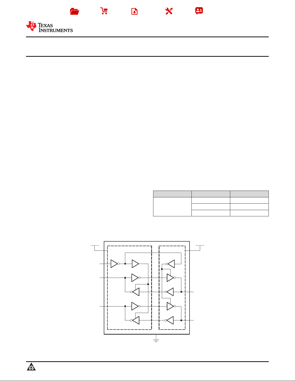
This 2-bit non-inverting bus transceiver uses two
separate configurable power-supply rails. The A ports
are designed to track V
and accepts any supply
CCA
voltage from 1.2 V to 3.6 V. The B ports are designed
to track V
and accepts any supply voltage from
CCB
1.2 V to 3.6 V. This allows for universal low-voltage
bidirectional translation and level-shifting between
any of the 1.2 V, 1.5 V, 1.8 V, 2.5 V, and 3.3 V
voltage nodes.
The SN74AVCH2T45 is designed for asynchronous
communication between two data buses. The logic
levels of the direction-control (DIR pin) input activate
either the B-port outputs or the A-port outputs. The
device transmits data from the A bus to the B bus
when the B-port outputs are activated and from the B
bus to the A bus when the A-port outputs are
activated. The SN74AVCH2T45 features active bushold circuitry, which holds unused or un-driven inputs
at a valid logic state. TI does not recommend using
pull-up or pull-down resistors with the bus-hold
circuitry.
Device Information
PART NUMBER PACKAGE BODY SIZE (NOM)
SSOP (8) 2.95 mm × 2.80 mm
SN74AVCH2T45 VSSOP (8) 2.30 mm × 2.00 mm
DSBGA (8) 1.89 mm × 0.89 mm
(1) For all available packages, see the orderable addendum at
the end of the data sheet.
(1)
Logic Diagram (Positive Logic)
1
An IMPORTANT NOTICE at the end of this data sheet addresses availability, warranty, changes, use in safety-critical applications,
intellectual property matters and other important disclaimers. PRODUCTION DATA.

SN74AVCH2T45
SCES582H –JULY 2004–REVISED APRIL 2015
www.ti.com
Table of Contents
1 Features.................................................................. 1 8 Parameter Measurement Information ................ 13
2 Applications ........................................................... 1 9 Detailed Description ............................................ 14
3 Description ............................................................. 1
4 Revision History..................................................... 3
5 Description (Continued)........................................ 4
6 Pin Configurations and Functions....................... 4
7 Specifications......................................................... 5
7.1 Absolute Maximum Ratings ...................................... 5
7.2 ESD Ratings.............................................................. 5
7.3 Recommended Operating Conditions ...................... 6
7.4 Thermal Information.................................................. 7
7.5 Electrical Characteristics .......................................... 7
7.6 Switching Characteristics: V
7.7 Switching Characteristics: V
7.8 Switching Characteristics: V
7.9 Switching Characteristics: V
7.10 Switching Characteristics: V
7.11 Operating Characteristics...................................... 11
7.12 Typical Characteristics.......................................... 12 14 Mechanical, Packaging, and Orderable
= 1.2 V ................... 8
CCA
= 1.5 V .................. 9
CCA
= 1.8 V ................. 10
CCA
= 2.5 V ................. 10
CCA
= 3.3 V ............... 11
CCA
9.1 Overview................................................................. 14
9.2 Functional Block Diagram....................................... 14
9.3 Feature Description................................................. 15
9.4 Device Functional Modes........................................ 15
10 Application and Implementation........................ 16
10.1 Application Information.......................................... 16
10.2 Typical Applications .............................................. 16
11 Power Supply Recommendations ..................... 20
12 Layout................................................................... 20
12.1 Layout Guidelines ................................................. 20
12.2 Layout Example .................................................... 20
13 Device and Documentation Support ................. 21
13.1 Documentation Support ....................................... 21
13.2 Trademarks........................................................... 21
13.3 Electrostatic Discharge Caution............................ 21
13.4 Glossary................................................................ 21
Information........................................................... 21
2 Submit Documentation Feedback Copyright © 2004–2015, Texas Instruments Incorporated
Product Folder Links: SN74AVCH2T45

SN74AVCH2T45
www.ti.com
SCES582H –JULY 2004–REVISED APRIL 2015
4 Revision History
Changes from Revision G (April 2015) to Revision H Page
• Added additional applications................................................................................................................................................. 1
• Updated Overview section. .................................................................................................................................................. 14
• Updated Layout Guidelines section. .................................................................................................................................... 20
Changes from Revision F (November 2007) to Revision G Page
• Added ESD Ratings table, Feature Description section, Device Functional Modes, Application and Implementation
section, Power Supply Recommendations section, Layout section, Device and Documentation Support section, and
Mechanical, Packaging, and Orderable Information section ................................................................................................. 1
Copyright © 2004–2015, Texas Instruments Incorporated Submit Documentation Feedback 3
Product Folder Links: SN74AVCH2T45
4
3
2
1
5
6
7
8
GND
A2
A1
V
CCA
DIR
B2
B1
V
CCB
D1 D2
C2C1
B1 B2
A1 A2
1
2
3
4
8
7
6
5
V
CCA
A1
A2
GND
V
CCB
B1
B2
DIR
SN74AVCH2T45
SCES582H –JULY 2004–REVISED APRIL 2015
www.ti.com
5 Description (Continued)
This device is fully specified for partial-power-down applications using I
preventing damaging current backflow through the device when it is powered down. The VCCisolation feature
ensures that if either VCCinput is at GND, then both outputs are in the high-impedance state. The bus-hold
circuitry on the powered-up side always stays active.
Active bus-hold circuitry holds unused or un-driven inputs at a valid logic state. NanoFree package technology is
a major breakthrough in IC packaging concepts, using the die as the package.
. The I
off
circuitry disables the outputs,
off
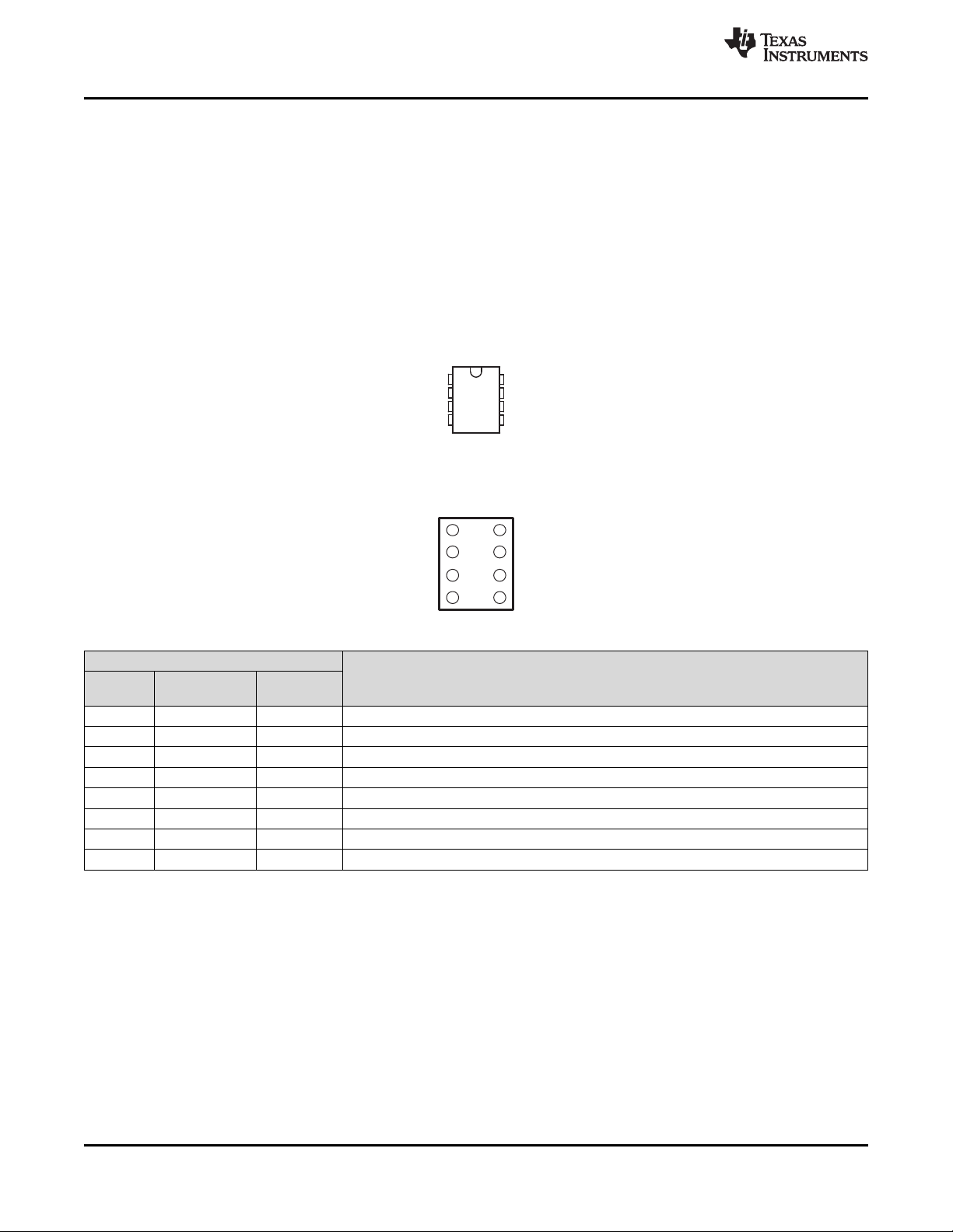
6 Pin Configurations and Functions
DCT and DCU Packages
8-Pin SSOP and VSSOP
Top View
YZP Package
8-Pin DSBGA
Bottom View
Pin Functions
PIN
NAME DSBGA
SSOP,
VSSOP
VCCA 1 A1 Supply Voltage A
VCCB 8 A2 Supply Voltage B
GND 4 D1 Ground
A1 2 B1 Output or input depending on state of DIR. Output level depends on V
A2 3 C1 Output or input depending on state of DIR. Output level depends on V
B1 7 B2 Output or input depending on state of DIR. Output level depends on V
B2 6 C2 Output or input depending on state of DIR. Output level depends on V
DIR 5 D2 Direction Pin, Connect to GND or to VCCA.
DESCRIPTION
CCA
CCA
CCB
CCB
.
.
.
.
4 Submit Documentation Feedback Copyright © 2004–2015, Texas Instruments Incorporated
Product Folder Links: SN74AVCH2T45
SN74AVCH2T45
www.ti.com
SCES582H –JULY 2004–REVISED APRIL 2015
7 Specifications
7.1 Absolute Maximum Ratings
(2)(3)
(1)
MIN MAX UNIT
I/O ports (A port) –0.5 4.6
I/O ports (B port) –0.5 4.6 V
Control inputs –0.5 4.6
A port –0.5 4.6
B port –0.5 4.6
A port –0.5 V
B port –0.5 V
CCA
CCB
+ 0.5
+ 0.5
V
V
over operating free-air temperature range (unless otherwise noted)
V
CCA
V
V
V
V
I
IK
I
OK
I
O
T
J
T
stg
(1) Stresses beyond those listed under Absolute Maximum Ratings may cause permanent damage to the device. These are stress ratings
(2) The input voltage and output negative-voltage ratings may be exceeded if the input and output current ratings are observed.
(3) The output positive-voltage rating may be exceeded up to 4.6 V maximum if the output current rating is observed.
Supply voltage –0.5 4.6 V
CCB
Input voltage
I
Voltage range applied to any output
O
in the high-impedance or power-off state
Voltage range applied to any output in the high or low state
O
(2)
(2)
Input clamp current VI< 0 –50 mA
Output clamp current VO< 0 –50 mA
Continuous output current ±50 mA
Continuous current through V
CCA
, V
, or GND ±100 mA
CCB
Junction temperature –40 150 °C
Storage temperature –65 150 °C
only, which do not imply functional operation of the device at these or any other conditions beyond those indicated under Recommended
Operating Conditions. Exposure to absolute-maximum-rated conditions for extended periods may affect device reliability.
7.2 ESD Ratings
Human body model (HBM), per ANSI/ESDA/JEDEC JS-001
V
(ESD)
Electrostatic discharge ±1000 V
Charged-device model (CDM), per JEDEC specification JESD22-
(2)
C101
Machine Model (MM), Per JEDEC specification JESD22-A115-A ±200
(1) JEDEC document JEP155 states that 500-V HBM allows safe manufacturing with a standard ESD control process.
(2) JEDEC document JEP157 states that 250-V CDM allows safe manufacturing with a standard ESD control process.
(1)
VALUE UNIT
±8000
Copyright © 2004–2015, Texas Instruments Incorporated Submit Documentation Feedback 5
Product Folder Links: SN74AVCH2T45
SN74AVCH2T45
SCES582H –JULY 2004–REVISED APRIL 2015
www.ti.com
7.3 Recommended Operating Conditions
over operating free-air temperature range (unless otherwise noted)
(4)
V
CCI
V
Supply voltage 1.2 3.6 V
CCA
V
Supply voltage 1.2 3.6 V
CCB
High-level
V
input Data inputs
IH
voltage
Low-level
V
input Data inputs
IL
voltage
(2)
(2)
High-level DIR
V
input (referenced to 1.95 V to 2.7 V 1.6 V
IH
voltage V
CCA
(3)
)
Low-level DIR
V
input (referenced to 1.95 V to 2.7 V 0.7 V
IL
voltage V
V
Input voltage 0 3.6 V
I
Output
V
O
voltage
I
High-level output current –8 mA
OH
I
Low-level output current 8 mA
OL
(3)
)
CCA
Active state 0 V
3-state 0 3.6
Δt/Δv Input transition rise or fall rate 5 ns/V
T
Operating free-air temperature –40 85 °C
A
(1) All unused data inputs of the device must be held at V
Implications of Slow or Floating CMOS Inputs, SCBA004.
(2) For V
(3) For V
(4) V
(5) V
values not specified in the data sheet, VIHmin = V
CCI
values not specified in the data sheet, VIHmin = V
CCI
is the voltage associated with the input port supply VCCA or VCCB.
CCI
is the voltage associated with the output port supply VCCA or VCCB.
CCO
1.2 V to 1.95 V V
1.95 V to 2.7 V 1.6 V
2.7 V to 3.6 V 2
1.2 V to 1.95 V V
1.95 V to 2.7 V 0.7 V
2.7 V to 3.6 V 0.8
1.2 V to 1.95 V V
2.7 V to 3.6 V 2
1.2 V to 1.95 V V
2.7 V to 3.6 V 0.8
1.4 V to 1.6 V –6
1.65 V to 1.95
2.3 V to 2.7 V –9
1.4 V to 1.6 V 6
1.65 V to 1.95
2.3 V to 2.7 V 9
or GND to ensure proper device operation. Refer to the TI application report,
CCI
CCI
CCA
(1)(2)(3)
(5)
V
CCO
MIN NOM MAX UNIT
(4)
× 0.65
CCI
CCI
× 0.65
CCA
CCA
(4)
× 0.35
× 0.35
CCO
1.2 V –3
V
3 V to 3.6 V –12
1.2 V 3
V
3 V to 3.6 V 12
× 0.7 V, VILmax = V
× 0.7 V, VILmax = V
CCI
CCA
× 0.3 V.
× 0.3 V.
(5)
V
6 Submit Documentation Feedback Copyright © 2004–2015, Texas Instruments Incorporated
Product Folder Links: SN74AVCH2T45
SN74AVCH2T45
www.ti.com
SCES582H –JULY 2004–REVISED APRIL 2015
7.4 Thermal Information
SN74AVCH2T45
THERMAL METRIC
(1)
DCT (SSOP) DCU (VSSOP) YZP (DSBGA) UNIT
8 PINS 8 PINS 8 PINS
R
θJA
R
θJC(top)
R
θJB
ψ
JT
ψ
JB
Junction-to-ambient thermal resistance 194.4 199.3 105.8
Junction-to-case (top) thermal resistance 124.7 76.2 1.6
Junction-to-board thermal resistance 106.8 80.6 10.8 °C/W
Junction-to-top characterization parameter 49.8 7.1 3.1
Junction-to-board characterization parameter 105.8 80.1 10.8
(1) For more information about traditional and new thermal metrics, see the IC Package Thermal Metrics application report, SPRA953.
7.5 Electrical Characteristics
over recommended operating free-air temperature range (unless otherwise noted)
PARAMETER TEST CONDITIONS V
IOH= –100 μA 1.2 V to 3.6 V 1.2 V to 3.6 V V
IOH= –3 mA 1.2 V 1.2 V 0.95
(3)
V
OH
IOH= –6 mA 1.4 V 1.4 V 1.05
IOH= –8 mA 1.65 V 1.65 V 1.2
VI= V
IH
IOH= –9 mA 2.3 V 2.3 V 1.75
IOH= –12 mA 3 V 3 V 2.3
IOL= 100 μA 1.2 V to 3.6 V 1.2 V to 3.6 V 0.2
IOL= 3 mA 1.2 V 1.2 V 0.15
(3)
V
OL
IOL= 6 mA 1.4 V 1.4 V 0.35
IOL= 8 mA 1.65 V 1.65 V 0.45
VI= V
IL
IOL= 9 mA 2.3 V 2.3 V 0.55
IOL= 12 mA 3 V 3 V 0.7
(3)
I
I
DIR input VI= V
or GND 1.2 V to 3.6 V 1.2 V to 3.6 V ±0.025 ±0.25 ±1 μA
CCA
VI= 0.42 V 1.2 V 1.2 V 25
VI= 0.49 V 1.4 V 1.4 V 15
(4)
I
BHL
VI= 0.58 V 1.65 V 1.65 V 25 μA
VI= 0.7 V 2.3 V 2.3 V 45
VI= 0.8 V 3.3 V 3.3 V 100
VI= 0.78 V 1.2 V 1.2 V –25
VI= 0.91 V 1.4 V 1.4 V –15
(5)
I
BHH
VI= 1.07 V 1.65 V 1.65 V –25 μA
VI= 1.6 V 2.3 V 2.3 V –45
VI= 2 V 3.3 V 3.3 V –100
(6)
I
BHLO
VI= 0 to V
CC
CCA
V
CCB
1.2 V 1.2 V 50
1.6 V 1.6 V 125
1.95 V 1.95 V 200 μA
2.7 V 2.7 V 300
3.6 V 3.6 V 500
TA= 25°C –40°C to 85°C
MIN TYP MAX MIN TYP MAX
(1)(2)
CCO
– 0.2
UNIT
V
V
(1) V
(2) V
(3) VOH: Output High Voltage; VOL: Output Low Voltage; II: Control Input Current.
(4) The bus-hold circuit can sink at least the minimum low sustaining current at VILmaximum. I
(5) The bus-hold circuit can source at least the minimum high sustaining current at VIHmininum. I
(6) An external driver must source at least I
is the voltage associated with the output port supply VCCA or VCCB.
CCO
is the voltage associated with the input port supply VCCA or VCCB.
CCI
GND and then raising it to VILmaximum.
to VCCand then lowering it to VIHminimum.
to switch this node from low to high.
BHLO
should be measured after lowering VINto
BHL
should be measured after raising V
BHH
IN
Copyright © 2004–2015, Texas Instruments Incorporated Submit Documentation Feedback 7
Product Folder Links: SN74AVCH2T45
SN74AVCH2T45
SCES582H –JULY 2004–REVISED APRIL 2015
Electrical Characteristics (continued)
over recommended operating free-air temperature range (unless otherwise noted)
PARAMETER TEST CONDITIONS V
CCA
1.2 V 1.2 V –50
1.6 V 1.6 V –125
(7)
I
BHHO
VI= 0 to V
CC
1.95 V 1.95 V –200 μA
2.7 V 2.7 V –300
3.6 V 3.6 V –500
A port 0 V 0 V to 3.6 V ±0.1 ±1 ±5
(8)
I
off
B port 0 V to 3.6 V 0 V ±0.1 ±1 ±5
B port 0 V 3.6 V ±0.5 ±2.5 ±5
(8)
I
OZ
A port 3.6 V 0 V ±0.5 ±2.5 ±5 μA
VIor VO= 0 to 3.6 V μA
VO= V
VI= V
CCO
CCI
or GND,
or GND
1.2 V to 3.6 V 1.2 V to 3.6 V 10
(8)
I
CCA
VI= V
or GND, IO= 0 0 V 3.6 V –2 μA
CCI
3.6 V 0 V 10
1.2 V to 3.6 V 1.2 V to 3.6 V 10
(8)
I
CCB
VI= V
or GND, IO= 0 0 V 3.6 V 10 μA
CCI
3.6 V 0 V –2
I
+ I
CCA
CCB
Control
C
i
inputs
C
A or B port VI= 3.3 V or GND 3.3 V 3.3 V 6 pF
io
(7) An external driver must sink at least I
(8) I
: Partial Power Down Output current; IOZ: Hi-Z Output Current; I
off
VI= V
or GND, IO= 0 1.2 V to 3.6 V 1.2 V to 3.6 V 20 μA
CCI
VI= 3.3 V or GND 3.3 V 3.3 V 2.5 pF
to switch this node from high to low.
BHHO
V
CCB
: Supply A Current; I
CCA
TA= 25°C –40°C to 85°C
MIN TYP MAX MIN TYP MAX
(1)(2)
: Supply B Current.
CCB
www.ti.com
UNIT
7.6 Switching Characteristics: V
over recommended operating free-air temperature range, V
PARAMETER UNIT
(1)
t
PLH
(1)
t
PHL
(1)
t
PLH
(1)
t
PHL
(1)
t
PHZ
(1)
t
PLZ
(1)
t
PHZ
(1)
t
PLZ
(1)(2)
t
PZH
(1)(2)
t
PZL
(1)(2)
t
PZH
(1)(2)
t
PZL
(1) t
: Low-to-high Propagation Delay; t
PLH
Propagation Delay; t
(2) The enable time is a calculated value derived using the formula shown in the Enable Times section.
FROM TO
(INPUT) (OUTPUT)
A B ns
B A ns
DIR A ns
DIR B ns
DIR A ns
DIR B ns
: Hi-Z-to-High Propagation Delay; t
PZH
PHL
= 1.2 V
CCA
= 1.2 V (see Figure 7)
CCA
V
= 1.2 V V
CCB
= 1.5 V V
CCB
= 1.8 V V
CCB
= 2.5 V V
CCB
TYP TYP TYP TYP TYP
3.1 2.6 2.4 2.2 2.2
3.1 2.6 2.4 2.2 2.2
3.4 3.1 3 2.9 2.9
3.4 3.1 3 2.9 2.9
5.2 5.2 5.1 5 4.8
5.2 5.2 5.1 5 4.8
5 4 3.8 2.8 3.2
5 4 3.8 2.8 3.2
8.4 7.1 6.8 5.7 6.1
8.4 7.1 6.8 5.7 6.1
8.3 7.8 7.5 7.2 7
8.3 7.8 7.5 7.2 7
: High-to-Low Propagation Delay; t
: Hi-Z-to-Low Propagation Delay
PZL
: High-to-Hi-Z Propagation Delay; t
PHZ
= 3.3 V
CCB
: Low-to-Hi-Z
PLZ
8 Submit Documentation Feedback Copyright © 2004–2015, Texas Instruments Incorporated
Product Folder Links: SN74AVCH2T45
www.ti.com
SN74AVCH2T45
SCES582H –JULY 2004–REVISED APRIL 2015
7.7 Switching Characteristics: V
over recommended operating free-air temperature range, V
PARAMETER UNIT
(1)
t
PLH
(1)
t
PHL
(1)
t
PLH
(1)
t
PHL
(1)
t
PHZ
(1)
t
PLZ
(1)
t
PHZ
(1)
t
PLZ
(1)(2)
t
PZH
(1)(2)
t
PZL
(1)(2)
t
PZH
(1)(2)
t
PZL
(1) t
: Low-to-high Propagation Delay; t
PLH
Propagation Delay; t
(2) The enable time is a calculated value derived using the formula shown in the Enable Times section.
FROM TO
(INPUT) (OUTPUT)
A B ns
B A ns
DIR A ns
DIR B ns
DIR A ns
DIR B ns
: Hi-Z-to-High Propagation Delay; t
PZH
PHL
= 1.5 V
CCA
= 1.5 V ± 0.1 V (see Figure 7)
CCA
V
= 1.5 V V
V
= 1.2 V
CCB
CCB
± 0.1 V ± 0.15 V ± 0.2 V ± 0.3 V
= 1.8 V V
CCB
= 2.5 V V
CCB
TYP MIN MAX MIN MAX MIN MAX MIN MAX
2.8 0.7 5.4 0.5 4.6 0.4 3.7 0.3 3.5
2.8 0.7 5.4 0.5 4.6 0.4 3.7 0.3 3.5
2.7 0.8 5.4 0.7 5.2 0.6 4.9 0.5 4.7
2.7 0.8 5.4 0.7 5.2 0.6 4.9 0.5 4.7
3.9 1.3 8.5 1.3 7.8 1.1 7.7 1.4 7.6
3.9 1.3 8.5 1.3 7.8 1.1 7.7 1.4 7.6
4.7 1.1 7 1.4 6.9 1.2 6.9 1.7 7.1
4.7 1.1 7 1.4 6.9 1.2 6.9 1.7 7.1
7.4 12.4 12.1 11.8 11.8
7.4 12.4 12.1 11.8 11.8
6.7 13.9 12.4 11.4 11.1
6.7 13.9 12.4 11.4 11.1
: High-to-Low Propagation Delay; t
: Hi-Z-to-Low Propagation Delay
PZL
: High-to-Hi-Z Propagation Delay; t
PHZ
= 3.3 V
CCB
: Low-to-Hi-Z
PLZ
Copyright © 2004–2015, Texas Instruments Incorporated Submit Documentation Feedback 9
Product Folder Links: SN74AVCH2T45
SN74AVCH2T45
SCES582H –JULY 2004–REVISED APRIL 2015
www.ti.com
7.8 Switching Characteristics: V
over recommended operating free-air temperature range, V
PARAMETER UNIT
(1)
t
PLH
(1)
t
PHL
(1)
t
PLH
(1)
t
PHL
(1)
t
PHZ
(1)
t
PLZ
(1)
t
PHZ
(1)
t
PLZ
(1)(2)
t
PZH
(1)(2)
t
PZL
(1)(2)
t
PZH
(1)(2)
t
PZL
(1) t
: Low-to-high Propagation Delay; t
PLH
Propagation Delay; t
(2) The enable time is a calculated value derived using the formula shown in the Enable Times section.
FROM TO
(INPUT) (OUTPUT)
A B ns
B A ns
DIR A ns
DIR B ns
DIR A ns
DIR B ns
: Hi-Z-to-High Propagation Delay; t
PZH
PHL
7.9 Switching Characteristics: V
over recommended operating free-air temperature range, V
PARAMETER UNIT
(1)
t
PLH
(1)
t
PHL
(1)
t
PLH
(1)
t
PHL
(1)
t
PHZ
(1)
t
PLZ
(1)
t
PHZ
(1)
t
PLZ
(1)(2)
t
PZH
(1)(2)
t
PZL
(1)(2)
t
PZH
(1)(2)
t
PZL
(1) t
: Low-to-high Propagation Delay; t
PLH
Propagation Delay; t
(2) The enable time is a calculated value derived using the formula shown in the Enable Times section.
FROM TO
(INPUT) (OUTPUT)
A B ns
B A ns
DIR A ns
DIR B ns
DIR A ns
DIR B ns
: Hi-Z-to-High Propagation Delay; t
PZH
PHL
= 1.8 V
CCA
= 1.8 V ± 0.15 V (see Figure 7)
CCA
V
= 1.5 V V
V
= 1.2 V
CCB
CCB
± 0.1 V ± 0.15 V ± 0.2 V ± 0.3 V
= 1.8 V V
CCB
= 2.5 V V
CCB
TYP MIN MAX MIN MAX MIN MAX MIN MAX
2.7 0.5 5.2 0.4 4.3 0.2 3.4 0.2 3.1
2.7 0.5 5.2 0.4 4.3 0.2 3.4 0.2 3.1
2.4 0.7 4.7 0.5 4.4 0.5 4 0.4 3.8
2.4 0.7 4.7 0.5 4.4 0.5 4 0.4 3.8
3.7 1.3 8.1 0.7 6.9 1.4 5.3 1.1 5.2
3.7 1.3 8.1 0.7 6.9 1.4 5.3 1.1 5.2
4.4 1.3 5.8 1.3 5.9 0.8 5.7 1.5 5.9
4.4 1.3 5.8 1.3 5.9 0.8 5.7 1.5 5.9
6.8 10.5 10.3 9.7 9.7
6.8 10.5 10.3 9.7 9.7
6.4 13.3 11.2 8.7 8.3
6.4 13.3 11.2 8.7 8.3
: High-to-Low Propagation Delay; t
: Hi-Z-to-Low Propagation Delay
PZL
= 2.5 V
CCA
= 2.5 V ± 0.2 V (see Figure 7)
CCA
V
= 1.5 V V
V
= 1.2 V
CCB
CCB
± 0.1 V ± 0.15 V ± 0.2 V ± 0.3 V
: High-to-Hi-Z Propagation Delay; t
PHZ
= 1.8 V V
CCB
= 2.5 V V
CCB
TYP MIN MAX MIN MAX MIN MAX MIN MAX
2.6 0.4 4.9 0.2 4 0.2 3 0.2 2.6
2.6 0.4 4.9 0.2 4 0.2 3 0.2 2.6
2.1 0.6 3.8 0.5 3.4 0.4 3 0.3 2.8
2.1 0.6 3.8 0.5 3.4 0.4 3 0.3 2.8
2.4 0.7 7.9 0.8 6.4 0.8 5 0.5 4.3
2.4 0.7 7.9 0.8 6.4 0.8 5 0.5 4.3
3.8 1 4.3 0.6 4.3 0.5 4.2 1.1 4.1
3.8 1 4.3 0.6 4.3 0.5 4.2 1.1 4.1
5.9 8.5 7.7 7.2 6.9
5.9 8.5 7.7 7.2 6.9
5 12.8 10.4 8 6.9
5 12.8 10.4 8 6.9
: High-to-Low Propagation Delay; t
: Hi-Z-to-Low Propagation Delay
PZL
: High-to-Hi-Z Propagation Delay; t
PHZ
= 3.3 V
CCB
: Low-to-Hi-Z
PLZ
= 3.3 V
CCB
: Low-to-Hi-Z
PLZ
10 Submit Documentation Feedback Copyright © 2004–2015, Texas Instruments Incorporated
Product Folder Links: SN74AVCH2T45
www.ti.com
SN74AVCH2T45
SCES582H –JULY 2004–REVISED APRIL 2015
7.10 Switching Characteristics: V
over recommended operating free-air temperature range, V
PARAMETER UNIT
(1)
t
PLH
(1)
t
PHL
(1)
t
PLH
(1)
t
PHL
(1)
t
PHZ
(1)
t
PLZ
(1)
t
PHZ
(1)
t
PLZ
(1)(2)
t
PZH
(1)(2)
t
PZL
(1)(2)
t
PZH
(1)(2)
t
PZL
(1) t
: Low-to-high Propagation Delay; t
PLH
Propagation Delay; t
(2) The enable time is a calculated value derived using the formula shown in the Enable Times section.
FROM TO
(INPUT) (OUTPUT)
A B ns
B A ns
DIR A ns
DIR B ns
DIR A ns
DIR B ns
: High-to-Low Propagation Delay; t
: Hi-Z-to-High Propagation Delay; t
PZH
PHL
= 3.3 V
CCA
= 3.3 V ± 0.3 V (see Figure 7)
CCA
V
= 1.5 V V
V
= 1.2 V
CCB
CCB
± 0.1 V ± 0.15 V ± 0.2 V ± 0.3 V
= 1.8 V V
CCB
= 2.5 V V
CCB
CCB
TYP MIN MAX MIN MAX MIN MAX MIN MAX
2.5 0.3 4.7 0.2 3.8 0.2 2.8 0.2 2.4
2.5 0.3 4.7 0.2 3.8 0.2 2.8 0.2 2.4
2.1 0.6 3.6 0.4 3.1 0.3 2.6 0.3 2.4
2.1 0.6 3.6 0.4 3.1 0.3 2.6 0.3 2.4
2.9 1.1 8 1 6.5 1.3 4.7 1.2 4
2.9 1.1 8 1 6.5 1.3 4.7 1.2 4
3.4 0.5 6.6 0.3 5.6 0.3 4.6 1.1 4.2
3.4 0.5 6.6 0.3 5.6 0.3 4.6 1.1 4.2
5.5 10.2 8.7 7.2 6.6
5.5 10.2 8.7 7.2 6.6
5.4 12.7 10.3 7.5 6.4
5.4 12.7 10.3 7.5 6.4
: High-to-Hi-Z Propagation Delay; t
: Hi-Z-to-Low Propagation Delay
PZL
PHZ
PLZ
= 3.3 V
: Low-to-Hi-Z
7.11 Operating Characteristics
TA= 25°C
V
= V
PARAMETER UNIT
A-port input,
pdA
B-port input,
B-port output
(1)
C
A-port output
A-port input,
pdB
B-port input,
B-port output
(1)
C
A-port output
TEST
CONDITIONS
CL= 0,
f = 10 MHz, pF
(2)
(2)
t
= t
f
= 1 ns
r
CL= 0,
f = 10 MHz, pF
(2)
(2)
t
= t
f
= 1 ns
r
CCA
V
= 1.2 V V
CCB
TYP TYP TYP TYP TYP
3 3 3 3 4
13 13 14 15 15
13 13 14 15 15
3 3 3 3 4
(1) Power dissipation capacitance per transceiver
(2) tr: Rise time; tf: Fall time
CCA
= 1.5 V V
CCB
= V
CCB
= V
CCA
= 1.8 V V
CCA
= 2.5 V V
CCB
= V
CCB
CCA
= 3.3 V
=
Copyright © 2004–2015, Texas Instruments Incorporated Submit Documentation Feedback 11
Product Folder Links: SN74AVCH2T45
 Loading...