

SN74AVCBH164245
16-BIT DUAL-SUPPLY BUS TRANSCEIVER
WITH CONFIGURABLE VOLTAGE TRANSLATION AND 3-STATE OUTPUTS
SCES393 – JUNE 2002
D
Member of the Texas Instruments
Widebus Family
D
DOC Circuitry Dynamically Changes
Output Impedance, Resulting in Noise
Reduction Without Speed Degradation
D
Dynamic Drive Capability Is Equivalent to
Standard Outputs With I
±24 mA at 2.5-V V
D
Control Inputs VIH/VIL Levels are
Referenced to V
D
If Either V
CC
CC
Voltage
CCB
Input Is at GND, Both Ports
and IOL of
OH
Are in the High-Impedance State
D
Overvoltage-Tolerant Inputs/Outputs Allow
Mixed-Voltage-Mode Data Communications
description
This 16-bit (dual-octal) noninverting bus transceiver uses two separate configurable power-supply rails. The
A-port is designed to track V
to track V
CCB
. V
accepts any supply voltage from 1.4 V to 3.6 V. This allows for universal low-voltage
CCB
bidirectional translation between any of the 1.5-V, 1.8-V, 2.5-V, and 3.3-V voltage nodes.
CCA
. V
accepts any supply voltage from 1.4 V to 3.6 V . The B-port is designed
CCA
D
I
Supports Partial-Power-Down Mode
off
Operation
D
Fully Configurable Dual-Rail Design Allows
Each Port to Operate Over the Full 1.4-V to
3.6-V Power Supply Range
D
Bus Hold on Data Inputs Eliminates the
Need for External Pullup/Pulldown
Resistors
D
Latch-Up Performance Exceeds 100 mA Per
JESD 78, Class II
D
ESD Protection Exceeds JESD 22
– 2000-V Human-Body Model (A114-A)
– 200-V Machine Model (A115-A)
– 1000-V Charged-Device Model (C101)
The SN74AVCBH164245 is designed for asynchronous communication between data buses. The device
transmits data from the A bus to the B bus or from the B bus to the A bus, depending on the logic level at the
direction-control (DIR) input. The output-enable (OE
) input can be used to disable the outputs so the buses are
effectively isolated.
The SN74AVCBH164245 is designed so that the control pins (1DIR, 2DIR, 1OE
V
.
CCB
, and 2OE) are supplied by
Active bus-hold circuitry is provided to hold unused or floating data inputs at a valid logic level. Use of pullup
or pulldown resistors with the bus-hold circuitry is not recommended.
T o ensure the high-impedance state during power up or power down, OE
should be tied to V
through a pullup
CCB
resistor; the minimum value of the resistor is determined by the current-sinking capability of the driver.
This device is fully specified for partial-power-down applications using I
off
. The I
preventing damaging current backflow through the device when it is powered down. If either V
circuitry disables the outputs,
off
input is at GND,
CC
both ports are in the high-impedance state.
Please be aware that an important notice concerning availability, standard warranty, and use in critical applications of
Texas Instruments semiconductor products and disclaimers thereto appears at the end of this data sheet.
DOC and Widebus are trademarks of Texas Instruments.
PRODUCTION DATA information is current as of publication date.
Products conform to specifications per the terms of Texas Instruments
standard warranty. Production processing does not necessarily include
testing of all parameters.
POST OFFICE BOX 655303 • DALLAS, TEXAS 75265
Copyright 2002, Texas Instruments Incorporated
1
SN74AVCBH164245
16-BIT DUAL-SUPPLY BUS TRANSCEIVER
WITH CONFIGURABLE VOLTAGE TRANSLATION AND 3-STATE OUTPUTS
SCES393 – JUNE 2002
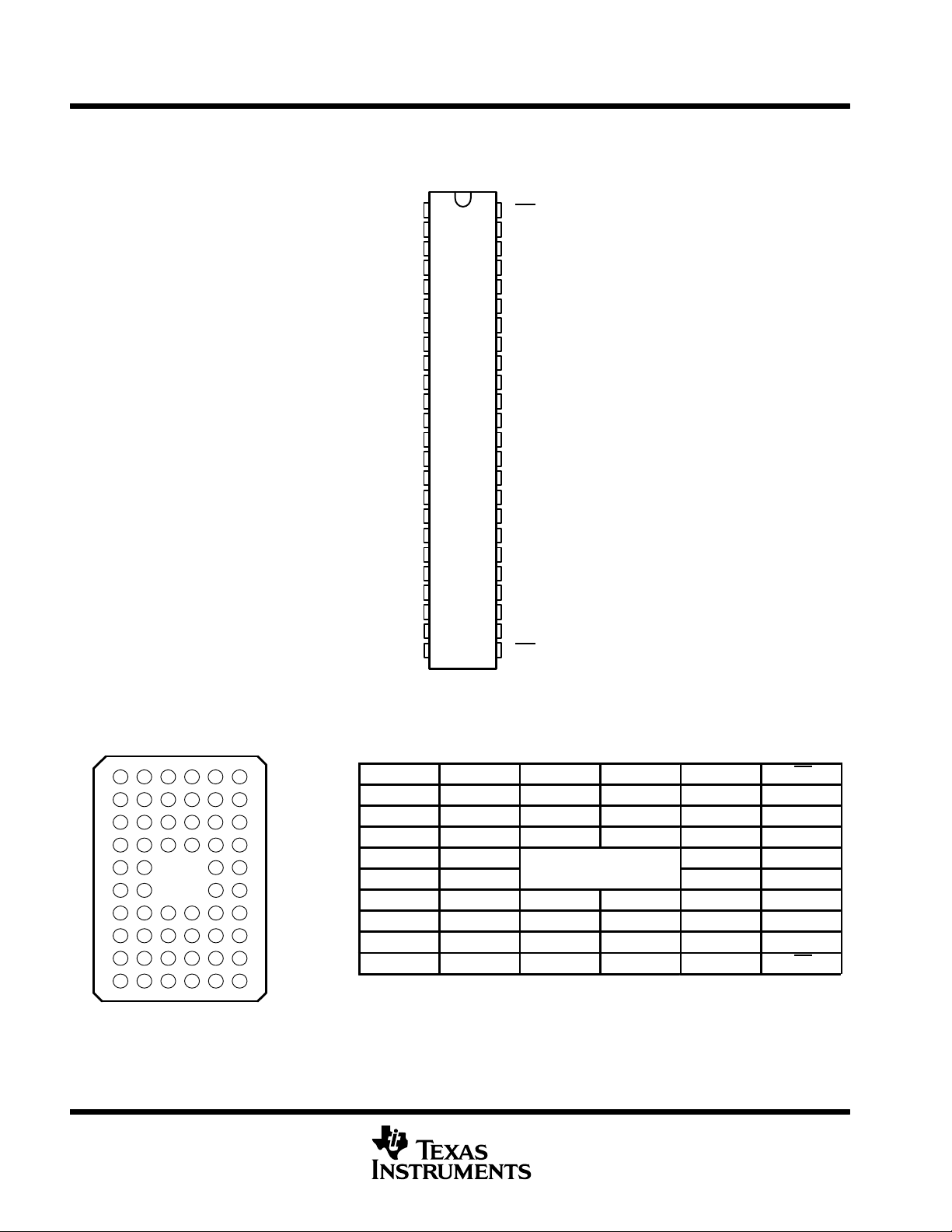
terminal assignments
DGG OR DGV PACKAGE
(TOP VIEW)
1
48
47
46
45
44
43
42
41
40
39
38
37
36
35
34
33
32
31
30
29
28
27
26
25
1OE
1A1
1A2
GND
1A3
1A4
V
CCA
1A5
1A6
GND
1A7
1A8
2A1
2A2
GND
2A3
2A4
V
CCA
2A5
2A6
GND
2A7
2A8
2OE
1DIR
1B1
1B2
GND
1B3
1B4
V
CCB
1B5
1B6
GND
1B7
1B8
2B1
2B2
GND
2B3
2B4
V
CCB
2B5
2B6
GND
2B7
2B8
2DIR
2
3
4
5
6
7
8
9
10
11
12
13
14
15
16
17
18
19
20
21
22
23
24
GQL PACKAGE
(TOP VIEW)
terminal assignments
213465
A
B
C
D
E
F
G
H
J
K
A 1DIR
B 1B2 1B1 GND GND 1A1 1A2
C 1B4 1B3 V
D 1B6 1B5 GND GND 1A5 1A6
E 1B8 1B7 1A7 1A8
F 2B1 2B2 2A2 2A1
G 2B3 2B4 GND GND 2A4 2A3
H 2B5 2B6 V
J 2B7 2B8 GND GND 2A8 2A7
K 2DIR NC NC NC NC 2OE
123456
NC NC NC NC 1OE
NC – No internal connection
CCB
CCB
V
V
CCA
CCA
1A3 1A4
2A6 2A5
2
POST OFFICE BOX 655303 • DALLAS, TEXAS 75265
OPERATION
WITH CONFIGURABLE VOLTAGE TRANSLATION AND 3-STATE OUTPUTS
T
A
TSSOP – DGG Tape and reel SN74AVCBH164245GR AVCBH164245
–40°C to 85°C
†
Package drawings, standard packing quantities, thermal data, symbolization, and PCB design guidelines
are available at www.ti.com/sc/package.
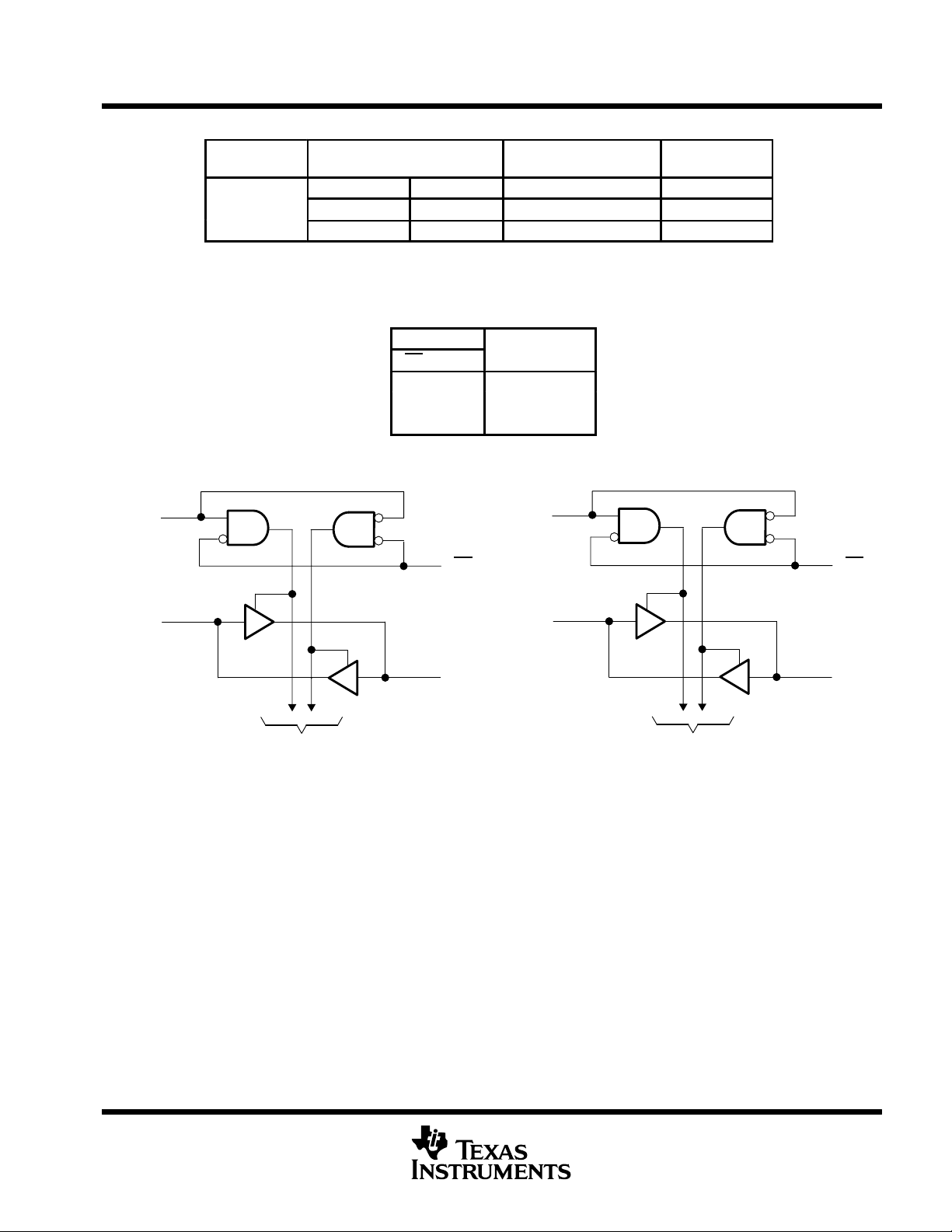
logic diagram (positive logic)
TVSOP – DGV Tape and reel SN74AVCBH164245VR WBH4245
VFBGA – GQL Tape and reel SN74AVCBH164245KR WBH4245
16-BIT DUAL-SUPPLY BUS TRANSCEIVER
ORDERING INFORMATION
PACKAGE
†
FUNCTION TABLE
(each 8-bit section)
INPUTS
DIR
OE
L L B data to A bus
L H A data to B bus
H X Isolation
ORDERABLE
PART NUMBER
SN74AVCBH164245
SCES393 – JUNE 2002
TOP-SIDE
MARKING
1
1DIR
47
1A1
To Seven Other Channels
Pin numbers shown are for the DGG and DGV packages.
48
24
2DIR
1OE
36
2A1
2
1B1
To Seven Other Channels
25
13
2OE
2B1
POST OFFICE BOX 655303 • DALLAS, TEXAS 75265
3

SN74AVCBH164245
16-BIT DUAL-SUPPLY BUS TRANSCEIVER
WITH CONFIGURABLE VOLTAGE TRANSLATION AND 3-STATE OUTPUTS
SCES393 – JUNE 2002
absolute maximum ratings over operating free-air temperature range (unless otherwise noted)
Supply voltage range, V
Input voltage range, V
Voltage range applied to any output in the high-impedance or power-off state, V
(see Note 1): (A port) –0.5 V to 4.6 V. . . . . . . . . . . . . . . . . . . . . . . . . . . . . . . . . . . . . . . . . . . . . . . . . . . . . . . . . . .
(B port) –0.5 V to 4.6 V. . . . . . . . . . . . . . . . . . . . . . . . . . . . . . . . . . . . . . . . . . . . . . . . . . . . . . . . . . .
Voltage range applied to any output in the high or low state, V
(see Notes 1 and 2): (A port) –0.5 V to V
Input clamp current, I
IK
Output clamp current, I
Continuous output current, I
Continuous current through V
Package thermal impedance, θ
Storage temperature range, T
†
Stresses beyond those listed under “absolute maximum ratings” may cause permanent damage to the device. These are stress ratings only, and
functional operation of the device at these or any other conditions beyond those indicated under “recommended operating conditions” is not
implied. Exposure to absolute-maximum-rated conditions for extended periods may affect device reliability.
NOTES: 1. The input voltage and output negative-voltage ratings may be exceeded if the input and output current ratings are observed.
2. The output positive-voltage rating may be exceeded up to 4.6 V maximum if the output current rating is observed.
3. The package thermal impedance is calculated in accordance with JESD 51-7.
and V
CCA
(see Note 1): I/O ports (A port) –0.5 V to 4.6 V. . . . . . . . . . . . . . . . . . . . . . . . . . . . . . . . .
I
–0.5 V to 4.6 V. . . . . . . . . . . . . . . . . . . . . . . . . . . . . . . . . . . . . . . . . . . . . .
CCB
I/O ports (B port) –0.5 V to 4.6 V. . . . . . . . . . . . . . . . . . . . . . . . . . . . . . . . .
Control inputs –0.5 V to 4.6 V. . . . . . . . . . . . . . . . . . . . . . . . . . . . . . . . . . .
O
O
(B port) –0.5 V to V
(VI < 0) –50 mA. . . . . . . . . . . . . . . . . . . . . . . . . . . . . . . . . . . . . . . . . . . . . . . . . . . . . . . . . . .
(VO < 0) –50 mA. . . . . . . . . . . . . . . . . . . . . . . . . . . . . . . . . . . . . . . . . . . . . . . . . . . . . . . .
OK
±50 mA. . . . . . . . . . . . . . . . . . . . . . . . . . . . . . . . . . . . . . . . . . . . . . . . . . . . . . . . . . . . .
O
CCA
JA
, V
, or GND ±100 mA. . . . . . . . . . . . . . . . . . . . . . . . . . . . . . . . . . . . . . . . .
CCB
(see Note 3): DGG package 70°C/W. . . . . . . . . . . . . . . . . . . . . . . . . . . . . . .
DGV package 58°C/W. . . . . . . . . . . . . . . . . . . . . . . . . . . . . . . .
GQL package 28°C/W. . . . . . . . . . . . . . . . . . . . . . . . . . . . . . . .
–65°C to 150°C. . . . . . . . . . . . . . . . . . . . . . . . . . . . . . . . . . . . . . . . . . . . . . . . . . .
stg
CCA
CCB
+ 0.5 V. . . . . . . . . . . . . . . . . . . . . . . . . . . . . . . . . . . . . . . . . . . .
+ 0.5 V. . . . . . . . . . . . . . . . . . . . . . . . . . . . . . . . . . . . . . . . . . . .
†
4
POST OFFICE BOX 655303 • DALLAS, TEXAS 75265

voltage
voltage
voltage
(Referenced to V
CCB
)
voltage
(Referenced to V
CCB
)
IOHHigh-level output current
mA
IOLLow-level output current
mA
SN74AVCBH164245
16-BIT DUAL-SUPPLY BUS TRANSCEIVER
WITH CONFIGURABLE VOLTAGE TRANSLATION AND 3-STATE OUTPUTS
SCES393 – JUNE 2002
recommended operating conditions (see Notes 4 through 6)
V
CCI
V
CCA
V
CCB
NOTES: 4. V
Supply voltage 1.4 3.6 V
Supply voltage 1.4 3.6 V
High-level input
V
IH
Low-level input
V
IL
High-level input
V
IH
Low-level input
V
IL
V
Output voltage 0 V
O
p
p
∆t/∆v Input transition rise or fall rate 5 ns/V
T
Operating free-air temperature –40 85 °C
A
is the VCC associated with the data input port.
CCI
5. V
6. All unused data inputs of the device must be held at V
is the VCC associated with the output port.
CCO
Implications of Slow or Floating CMOS Inputs, literature number SCBA004.
Data inputs
Data inputs
Control inputs
Control inputs
1.4 V to 1.95 V V
1.95 V to 2.7 V 1.7 V
2.7 V to 3.6 V 2 V
1.4 V to 1.95 V 0 V
1.95 V to 2.7 V 0 0.7
2.7 V to 3.6 V 0 0.8
1.4 V to 1.95 V V
1.95 V to 2.7 V 1.7 V
2.7 V to 3.6 V 2 V
1.4 V to 1.95 V 0 V
1.95 V to 2.7 V 0 0.7
2.7 V to 3.6 V 0 0.8
or GND to ensure proper device operation. Refer to the TI application report,
CCI
V
CCO
1.4 V to 1.6 V –2
1.65 V to 1.95 V –4
2.3 V to 2.7 V –8
3 V to 3.6 V –12
1.4 V to 1.6 V 2
1.65 V to 1.95 V 4
2.3 V to 2.7 V 8
3 V to 3.6 V 12
MIN MAX UNIT
× 0.65 V
CCI
× 0.65 V
CCB
CCI
CCB
CCI
CCI
CCI
× 0.35
CCB
CCB
CCB
× 0.35
CCO
V
V
V
V
V
POST OFFICE BOX 655303 • DALLAS, TEXAS 75265
5

SN74AVCBH164245
I
‡
A
I
§
A
I
¶
V
0 to V
A
I
#
V
0 to V
A
o
V
or V
0 to 3.6 V
A
16-BIT DUAL-SUPPLY BUS TRANSCEIVER
WITH CONFIGURABLE VOLTAGE TRANSLATION AND 3-STATE OUTPUTS
SCES393 – JUNE 2002
electrical characteristics over recommended operating free-air temperature range (unless
otherwise noted) (see Note 7)
PARAMETER TEST CONDITIONS
IOH = –100 µA VI = V
IOH = –2 mA VI = V
V
OH
V
OL
I
Control inputs VI = V
I
BHL
BHH
BHLO
BHHO
I
A port
o
f
B port
f
†
All typical values are at TA = 25°C.
‡
The bus-hold circuit can sink at least the minimum low sustaining current at VIL max. I
then raising it to VIL max.
§
The bus-hold circuit can source at least the minimum high sustaining current at VIH min. I
then lowering it to VIH min.
¶
An external driver must source at least I
#
An external driver must sink at least I
NOTE 7: V
CCO
IOH = –4 mA VI = V
IOH = –8 mA VI = V
IOH = –12 mA VI = V
IOH = 100 µA VI = V
IOH = 2 mA VI = V
IOH = 4 mA VI = V
IOH = 8 mA VI = V
IOH = 12 mA VI = V
or GND 1.4 V to 3.6 V 3.6 V ±2.5 µA
CCB
VI = 0.49 V 1.4 V 1.4 V 11
VI = 0.57 V 1.65 V 1.65 V 25
VI = 0.7 V 2.3 V 2.3 V 45
VI = 0.8 V 3 V 3 V 75
VI = 0.49 V 1.4 V 1.4 V –11
VI = 1.07 V 1.65 V 1.65 V –25
VI = 1.7 V 2.3 V 2.3 V –45
VI = 2 V 3 V 3 V –75
=
I
=
I
I
is the VCC associated with the output port.
CC
CC
=
O
BHLO
BHHO
IH
IH
IH
IH
IH
IL
IL
IL
IL
IL
to switch this node from low to high.
to switch this node from high to low.
V
CCA
1.4 V to 3.6 V 1.4 V to 3.6 V V
1.4 V 1.4 V 1.05
1.65 V 1.65 V 1.2
2.3 V 2.3 V 1.75
3 V 3 V 2.3
1.4 V to 3.6 V 1.4 V to 3.6 V 0.2
1.4 V 1.4 V 0.35
1.65 V 1.65 V 0.45
2.3 V 2.3 V 0.55
3 V 3 V 0.7
1.6 V 1.6 V 100
1.95 V 1.95 V 200
2.7 V 2.7 V 300
3.6 V 3.6 V 525
1.6 V 1.6 V –100
1.95 V 1.95 V –200
2.7 V 2.7 V –300
3.6 V 3.6 V –525
0 V 0 to 3.6 V ±10
0 to 3.6 V 0 V ±10
V
CCB
should be measured after lowering VIN to GND and
BHL
should be measured after raising VIN to VCC and
BHH
MIN TYP†MAX UNIT
–0.2 V
CCO
V
V
µ
µ
µ
µ
µ
6
POST OFFICE BOX 655303 • DALLAS, TEXAS 75265

‡
V
I
V
CCI
GND
OE
I
V
V
or GND
I
0
A
I
V
V
or GND
I
0
A
(INPUT)
(OUTPUT)
t
ns
t
ns
t
ns
SN74AVCBH164245
16-BIT DUAL-SUPPLY BUS TRANSCEIVER
WITH CONFIGURABLE VOLTAGE TRANSLATION AND 3-STATE OUTPUTS
SCES393 – JUNE 2002
electrical characteristics over recommended operating free-air temperature range (continued)
(unless otherwise noted) (see Notes 8 and 9)
PARAMETER TEST CONDITIONS
,
,
OE = V
= don’t care
=
O
=
O
A or B ports
I
OZ
CCA
CCB
C
i
C
io
†
All typical values are at TA = 25°C.
‡
For I/O ports, the parameter IOZ includes the input leakage current.
NOTES: 8. V
9. V
B port
A port
Control inputs VI = 3.3 V or GND 3.3 V 3.3 V 4 pF
A or B ports VO = 3.3 V or GND 3.3 V 3.3 V 5 pF
is the VCC associated with the output port.
CCO
is the VCC associated with the input port.
CCI
VO = V
=
=
=
I
=
I
CCO
CCI
CCI
or GND,
or
V
CCA
IH
3.6 V 3.6 V ±12.5
0 V 3.6 V ±12.5
3.6 V 0 V ±12.5
1.6 V 1.6 V 20
1.95 V 1.95 V 20
2.7 V 2.7 V 30
0 V 3.6 V –40
3.6 V 0 V 40
3.6 V 3.6 V 40
1.6 V 1.6 V 20
1.95 V 1.95 V 20
2.7 V 2.7 V 30
0 V 3.6 V 40
3.6 V 0 V –40
3.6 V 3.6 V 40
V
CCB
MIN TYP†MAX UNIT
µA
µ
µ
switching characteristics over recommended operating free-air temperature range,
= 1.5 V ± 0.1 V (see Figure 2)
V
CCA
V
PARAMETER
pd
en
dis
= 1.5 V
FROM
A B 1.7 6.7 1.9 6.3 1.8 5.5 1.7 5.8
B A 1.8 6.8 2.2 7.4 2.1 7.6 2.1 7.3
OE
OE
OE
OE
TO
A 2.5 8.4 2.4 7.4 2.1 5.2 1.9 4.2
B 2.1 9 2.9 9.8 3.2 10 3 9.8
A 2.2 6.9 2.3 6.1 1.3 3.6 1.3 3
B 2.1 7.1 2.3 6.4 1.7 5.1 1.6 4.8
CCB
± 0.1 V
MIN MAX MIN MAX MIN MAX MIN MAX
V
CCB
= 1.8 V
± 0.15 V
V
CCB
± 0.2 V
= 2.5 V
V
CCB
± 0.3 V
= 3.3 V
UNIT
POST OFFICE BOX 655303 • DALLAS, TEXAS 75265
7

SN74AVCBH164245
(INPUT)
(OUTPUT)
t
ns
t
ns
t
ns
(INPUT)
(OUTPUT)
t
ns
t
ns
t
ns
(INPUT)
(OUTPUT)
t
ns
t
ns
t
ns
16-BIT DUAL-SUPPLY BUS TRANSCEIVER
WITH CONFIGURABLE VOLTAGE TRANSLATION AND 3-STATE OUTPUTS
SCES393 – JUNE 2002
switching characteristics over recommended operating free-air temperature range,
V
switching characteristics over recommended operating free-air temperature range,
V
= 1.8 V ± 0.15 V (see Figure 2)
CCA
PARAMETER
pd
en
dis
= 2.5 V ± 0.2 V (see Figure 2)
CCA
PARAMETER
pd
en
dis
FROM
A B 1.7 6.4 1.8 6 1.7 4.7 1.6 4.3
B A 1.4 5.5 1.8 6 1.8 5.8 1.8 5.5
OE
OE
OE
OE
FROM
A B 1.6 6 1.8 5.6 1.5 4 1.4 3.4
B A 1.3 4.6 1.7 4.4 1.5 4 1.4 3.7
OE
OE
OE
OE
V
= 1.5 V
TO
A 2.6 8.5 2.5 7.5 2.2 5.3 1.9 4.2
B 1.8 7.6 2.6 7.7 2.6 7.6 2.6 7.4
A 2.3 7 2.3 6.1 1.3 3.6 1.3 3
B 1.8 7 2.5 6.3 1.8 4.7 1.7 4.4
TO
A 3.1 8.5 2.5 7.5 2.2 5.3 1.9 4.2
B 1.7 5.7 2.2 5.5 2.2 5.3 2.2 5.1
A 2.4 7 3 6.1 1.4 3.6 1.2 3
B 1.2 5.8 1.9 5 1.4 3.6 1.3 3.3
CCB
± 0.1 V
MIN MAX MIN MAX MIN MAX MIN MAX
V
= 1.5 V
CCB
± 0.1 V
MIN MAX MIN MAX MIN MAX MIN MAX
V
CCB
± 0.15 V
V
CCB
± 0.15 V
= 1.8 V
= 1.8 V
V
V
CCB
± 0.2 V
CCB
± 0.2 V
= 2.5 V
= 2.5 V
V
V
CCB
± 0.3 V
CCB
± 0.3 V
= 3.3 V
UNIT
= 3.3 V
UNIT
switching characteristics over recommended operating free-air temperature range,
= 3.3 V ± 0.3 V (see Figure 2)
V
CCA
V
PARAMETER
pd
en
dis
= 1.5 V
FROM
A B 1.5 5.9 1.7 5.4 1.5 3.7 1.4 3.1
B A 1.3 4.5 1.6 3.8 1.5 3.3 1.4 3.1
OE
OE
OE
OE
TO
A 2.6 8.3 2.5 7.4 2.2 5.2 1.9 4.1
B 1.6 4.9 2 4.5 2 4.3 1.9 4.1
A 2.3 7 3 6 1.3 3.5 1.2 3.5
B 1.3 6.9 2.1 5.5 1.6 3.8 1.5 3.5
CCB
± 0.1 V
MIN MAX MIN MAX MIN MAX MIN MAX
V
CCB
± 0.15 V
= 1.8 V
V
CCB
± 0.2 V
= 2.5 V
V
CCB
± 0.3 V
= 3.3 V
UNIT
8
POST OFFICE BOX 655303 • DALLAS, TEXAS 75265

dA
C
L
MHz
F
dB
C
0
MHz
pF
,
SN74AVCBH164245
16-BIT DUAL-SUPPLY BUS TRANSCEIVER
WITH CONFIGURABLE VOLTAGE TRANSLATION AND 3-STATE OUTPUTS
SCES393 – JUNE 2002
operating characteristics, V
Power dissipation capacitance per transceiver,
C
(V
C
(V
A port input, B port output
pdA
)
CCA
Power dissipation capacitance per transceiver,
B port input, A port output
Power dissipation capacitance per transceiver,
A port input, B port output
pdB
)
CCB
Power dissipation capacitance per transceiver,
B port input, A port output
and V
CCA
PARAMETER
CCB
= 3.3 V, T
Outputs enabled 14
Outputs disabled
Outputs enabled
Outputs disabled 7
Outputs enabled 20
Outputs disabled
Outputs enabled
Outputs disabled 7
= 25°C
A
TEST CONDITIONS TYP UNIT
= 0,f = 10
,f = 10
=
L
output description
The DOC circuitry is implemented, which, during the transition, initially lowers the output impedance to
effectively drive the load and, subsequently, raises the impedance to reduce noise. Figure 1 shows typical V
vs IOL and VOH vs IOH curves to illustrate the output impedance and drive capability of the circuit. At the
beginning of the signal transition, the DOC circuit provides a maximum dynamic drive that is equivalent to a
high-drive standard-output device. For more information, refer to the TI application reports, A VC Logic Family
Technology and Applications, literature number SCEA006, and Dynamic Output Control (DOC ) Circuitry
Technology and Applications, literature number SCEA009.
3.2
2.8
2.4
2.0
1.6
1.2
– Output Voltage – V
OL
0.8
V
0.4
TA = 25°C
Process = Nominal
VCC = 1.8 V
IOL – Output Current – mA
VCC = 2.5 V
VCC = 3.3 V
136
17015311910285685134170
2.8
2.4
2.0
1.6
1.2
– Output Voltage – V
OH
0.8
V
0.4
TA = 25°C
Process = Nominal
VCC = 3.3 V
–128–144–160
IOH – Output Current – mA
VCC = 2.5 V
VCC = 1.8 V
–80–96–112 –32–48–64 0–16
20
14
7
p
7
p
OL
Figure 1. Typical Output Voltage vs Output Current
POST OFFICE BOX 655303 • DALLAS, TEXAS 75265
9

SN74AVCBH164245
16-BIT DUAL-SUPPLY BUS TRANSCEIVER
WITH CONFIGURABLE VOLTAGE TRANSLATION AND 3-STATE OUTPUTS
SCES393 – JUNE 2002
PARAMETER MEASUREMENT INFORMATION
2 × V
From Output
Under Test
(see Note A)
CCO
R
L
C
L
R
L
S1
Open
GND
TEST S1
t
pd
t
PLZ/tPZL
t
PHZ/tPZH
Open
2 × V
GND
CCO
1.5 V ± 0.1 V
1.8 V ± 0.15 V
2.5 V ± 0.2 V
3.3 V ± 0.3 V
Input
t
Output
LOAD CIRCUIT
V
CCO
PLH
PROPAGATION DELAY TIMES
C
L
15 pF
30 pF
30 pF
30 pF
V
/2 V
CCI
VOLTAGE WAVEFORMS
V
/2 V
CCO
R
2 kΩ
1 kΩ
500 Ω
500 Ω
t
w
V
CCI
V
V
CCI
0.1 V
0.15 V
0.15 V
0.3 V
/2
TP
t
PHL
CCO
/2
V
0 V
V
V
CCI
OH
OL
L
Input
Control
(low-level
enabling)
Output
Waveform 1
S1 at 2 × V
(see Note B)
Output
Waveform 2
S1 at GND
(see Note B)
Output
CCO
t
PZL
t
PZH
ENABLE AND DISABLE TIMES
/2 V
CCI
VOLTAGE WAVEFORMS
PULSE DURATION
/2
CCB
V
CCO
V
CCO
VOLTAGE WAVEFORMS
V
/2
/2
CCI
CCB
VOL + V
VOH – V
/2V
t
t
PHZ
/2
PLZ
TP
TP
0 V
V
0 V
V
V
V
0 V
CCB
CCO
OL
OH
NOTES: A. CL includes probe and jig capacitance.
B. Waveform 1 is for an output with internal conditions such that the output is low except when disabled by the output control.
Waveform 2 is for an output with internal conditions such that the output is high except when disabled by the output control.
C. All input pulses are supplied by generators having the following characteristics: PRRv10 MHz, ZO = 50 Ω, dv/dt ≥1 V/ns,
dv/dt ≥1 V/ns.
D. The outputs are measured one at a time with one transition per measurement.
E. t
F. t
G. t
H. V
I. V
and t
PLZ
and t
PZL
and t
PLH
is the VCC associated with the input port.
CCI
CCO
are the same as t
PHZ
are the same as ten.
PZH
are the same as tpd.
PHL
is the VCC associated with the output port.
dis
Figure 2. Load Circuit and Voltage Waveforms
10
POST OFFICE BOX 655303 • DALLAS, TEXAS 75265
.

IMPORTANT NOTICE
Texas Instruments Incorporated and its subsidiaries (TI) reserve the right to make corrections, modifications,
enhancements, improvements, and other changes to its products and services at any time and to discontinue
any product or service without notice. Customers should obtain the latest relevant information before placing
orders and should verify that such information is current and complete. All products are sold subject to TI’s terms
and conditions of sale supplied at the time of order acknowledgment.
TI warrants performance of its hardware products to the specifications applicable at the time of sale in
accordance with TI’s standard warranty . Testing and other quality control techniques are used to the extent TI
deems necessary to support this warranty . Except where mandated by government requirements, testing of all
parameters of each product is not necessarily performed.
TI assumes no liability for applications assistance or customer product design. Customers are responsible for
their products and applications using TI components. T o minimize the risks associated with customer products
and applications, customers should provide adequate design and operating safeguards.
TI does not warrant or represent that any license, either express or implied, is granted under any TI patent right,
copyright, mask work right, or other TI intellectual property right relating to any combination, machine, or process
in which TI products or services are used. Information published by TI regarding third–party products or services
does not constitute a license from TI to use such products or services or a warranty or endorsement thereof.
Use of such information may require a license from a third party under the patents or other intellectual property
of the third party , or a license from TI under the patents or other intellectual property of TI.
Reproduction of information in TI data books or data sheets is permissible only if reproduction is without
alteration and is accompanied by all associated warranties, conditions, limitations, and notices. Reproduction
of this information with alteration is an unfair and deceptive business practice. TI is not responsible or liable for
such altered documentation.
Resale of TI products or services with statements different from or beyond the parameters stated by TI for that
product or service voids all express and any implied warranties for the associated TI product or service and
is an unfair and deceptive business practice. TI is not responsible or liable for any such statements.
Mailing Address:
Texas Instruments
Post Office Box 655303
Dallas, Texas 75265
Copyright 2002, Texas Instruments Incorporated
 Loading...