

Page 1
www.ti.com
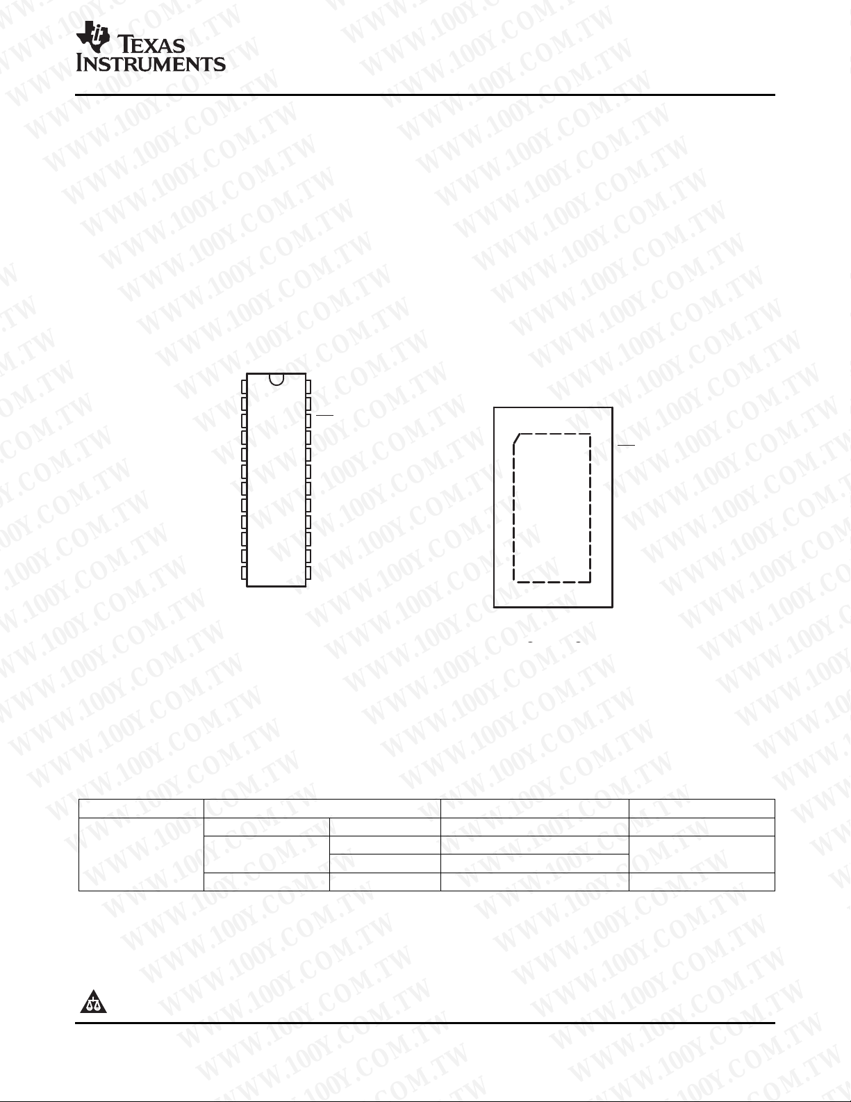
DGV OR PW PACKAGE
(TOP VIEW)
1
2
3
4
5
6
7
8
9
10
11
12
24
23
22
21
20
19
18
17
16
15
14
13
V
CCA
DIR
A1
A2
A3
A4
A5
A6
A7
A8
GND
GND
V
CCB
V
CCB
OE
B1
B2
B3
B4
B5
B6
B7
B8
GND
RHL PACKAGE
(TOP VIEW)
1 24
12 13
2
3
4
5
6
7
8
9
10
11
23
22
21
20
19
18
17
16
15
14
V
CCB
OE
B1
B2
B3
B4
B5
B6
B7
B8
DIR
A1
A2
A3
A4
A5
A6
A7
A8
GND
GND
V
GND
CCB
V
CCA
SN74AVC8T245
8-BIT DUAL-SUPPLY BUS TRANSCEIVER
WITH CONFIGURABLE VOLTAGE TRANSLATION AND 3-STATE OUTPUTS
SCES517H – DECEMBER 2003 – REVISED FEBRUARY 2007
FEATURES
• Control Inputs V
• V
to V
CC
Voltage
CCA
Isolation Feature – If Either V
/V
Levels Are Referenced • Max Data Rates
IH
IL
GND, All I/O Ports Are in the High-Impedance
State
• I
Supports Partial Power-Down-Mode
off
Operation
• Fully Configurable Dual-Rail Design Allows
Each Port to Operate Over the Full 1.4-V to
3.6-V Power-Supply Range
• I/Os Are 4.6-V Tolerant
CC
Input Is at
– 170 Mbps (V
– 320 Mbps (V
< 1.8 V or V
CCA
≥ 1.8 V and V
CCA
CCB
CCB
• Latch-Up Performance Exceeds 100 mA Per
JESD 78, Class II
• ESD Protection Exceeds JESD 22
– 8000-V Human-Body Model (A114-A)
– 200-V Machine Model (A115-A)
– 1000-V Charged-Device Model (C101)
< 1.8 V)
≥ 1.8 V)
DESCRIPTION/ORDERING INFORMATION
This 8-bit noninverting bus transceiver uses two separate configurable power-supply rails. The SN74AVC8T245
is optimized to operate with V
A port is designed to track V
WWW.100Y.COM.TW WWW.100Y.COM.TW WWW.100Y.COM.TW
bidirectional translation between any of the 1.2-V, 1.5-V, 1.8-V, 2.5-V, and 3.3-V voltage nodes.
track V
. V
CCB
accepts any supply voltage from 1.2 V to 3.6 V. This allows for universal low-voltage
CCB
WWW.100Y.COM.TW WWW.100Y.COM.TW WWW.100Y.COM.TW
WWW.100Y.COM.TW WWW.100Y.COM.TW WWW.100Y.COM.TW
WWW.100Y.COM.TW WWW.100Y.COM.TW WWW.100Y.COM.TW
–40 ° C to 85 ° C TSSOP – PW WE245
WWW.100Y.COM.TW WWW.100Y.COM.TW WWW.100Y.COM.TW
(1) For the most current package and ordering information, see the Package Option Addendum at the end of this document, or see the TI
PRODUCTION DATA information is current as of publication date.
Products conform to specifications per the terms of the Texas
Instruments standard warranty. Production processing does not
necessarily include testing of all parameters.
T
A
QFN – RHL Reel of 1000 SN74AVC8T245RHLR WE245
WWW.100Y.COM.TW WWW.100Y.COM.TW WWW.100Y.COM.TW
website at www.ti.com .
WWW.100Y.COM.TW WWW.100Y.COM.TW WWW.100Y.COM.TW
WWW.100Y.COM.TW WWW.100Y.COM.TW WWW.100Y.COM.TW
Please be aware that an important notice concerning availability, standard warranty, and use in critical applications of Texas
Instruments semiconductor products and disclaimers thereto appears at the end of this data sheet.
TVSOP – DGV Reel of 2000 SN74AVC8T245DGVR WE245
WWW.100Y.COM.TW WWW.100Y.COM.TW WWW.100Y.COM.TW
WWW.100Y.COM.TW WWW.100Y.COM.TW WWW.100Y.COM.TW
CCA
CCA
/V
set at 1.4 V to 3.6 V. It is operational with V
CCB
. V
accepts any supply voltage from 1.2 V to 3.6 V. The B port is designed to
CCA
/V
CCA
as low as 1.2 V. The
CCB
ORDERING INFORMATION
PACKAGE
(1)
Tube of 60 SN74AVC8T245PW
Reel of 2000 SN74AVC8T245PWR
ORDERABLE PART NUMBER TOP-SIDE MARKING
Copyright © 2003–2007, Texas Instruments Incorporated
WWW.100Y.COM.TW WWW.100Y.COM.TW WWW.100Y.COM.TW
Page 2
www.ti.com
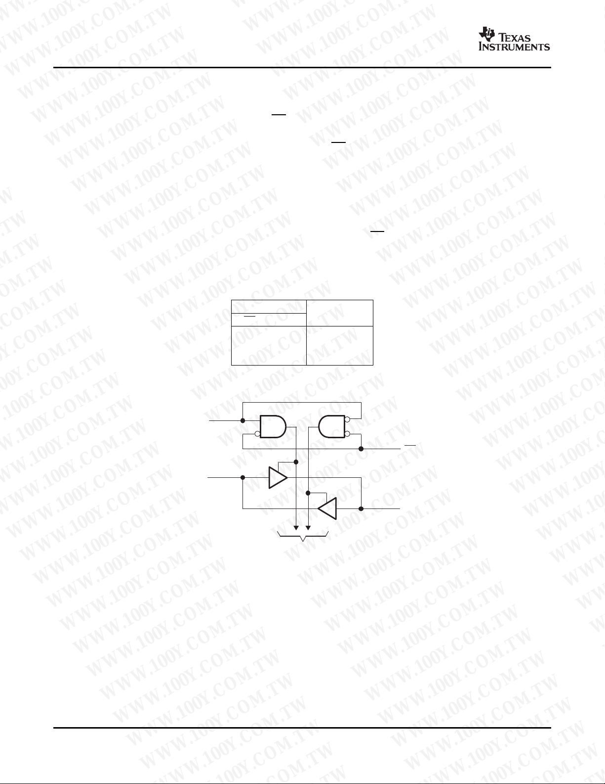
DIR
OE
A1
B1
To Seven Other Channels
2
3
22
21
SN74AVC8T245
8-BIT DUAL-SUPPLY BUS TRANSCEIVER
WITH CONFIGURABLE VOLTAGE TRANSLATION AND 3-STATE OUTPUTS
SCES517H – DECEMBER 2003 – REVISED FEBRUARY 2007
DESCRIPTION/ORDERING INFORMATION (CONTINUED)
The SN74AVC8T245 is designed for asynchronous communication between data buses. The device transmits
data from the A bus to the B bus or from the B bus to the A bus, depending on the logic level at the
direction-control (DIR) input. The output-enable ( OE) input can be used to disable the outputs so the buses are
effectively isolated.
The SN74AVC8T245 is designed so the control pins (DIR and OE) are supplied by V
The SN74AVC8T245 solution is compatible with a single-supply system and can be replaced later with a '245
function, with minimal printed circuit board redesign.
This device is fully specified for partial-power-down applications using I
preventing damaging current backflow through the device when it is powered down.
The V
To ensure the high-impedance state during power up or power down, OE shall be tied to V
resistor; the minimum value of the resistor is determined by the current-sinking capability of the driver.
isolation feature ensures that if either V
CC
input is at GND, both ports are in the high-impedance state.
CC
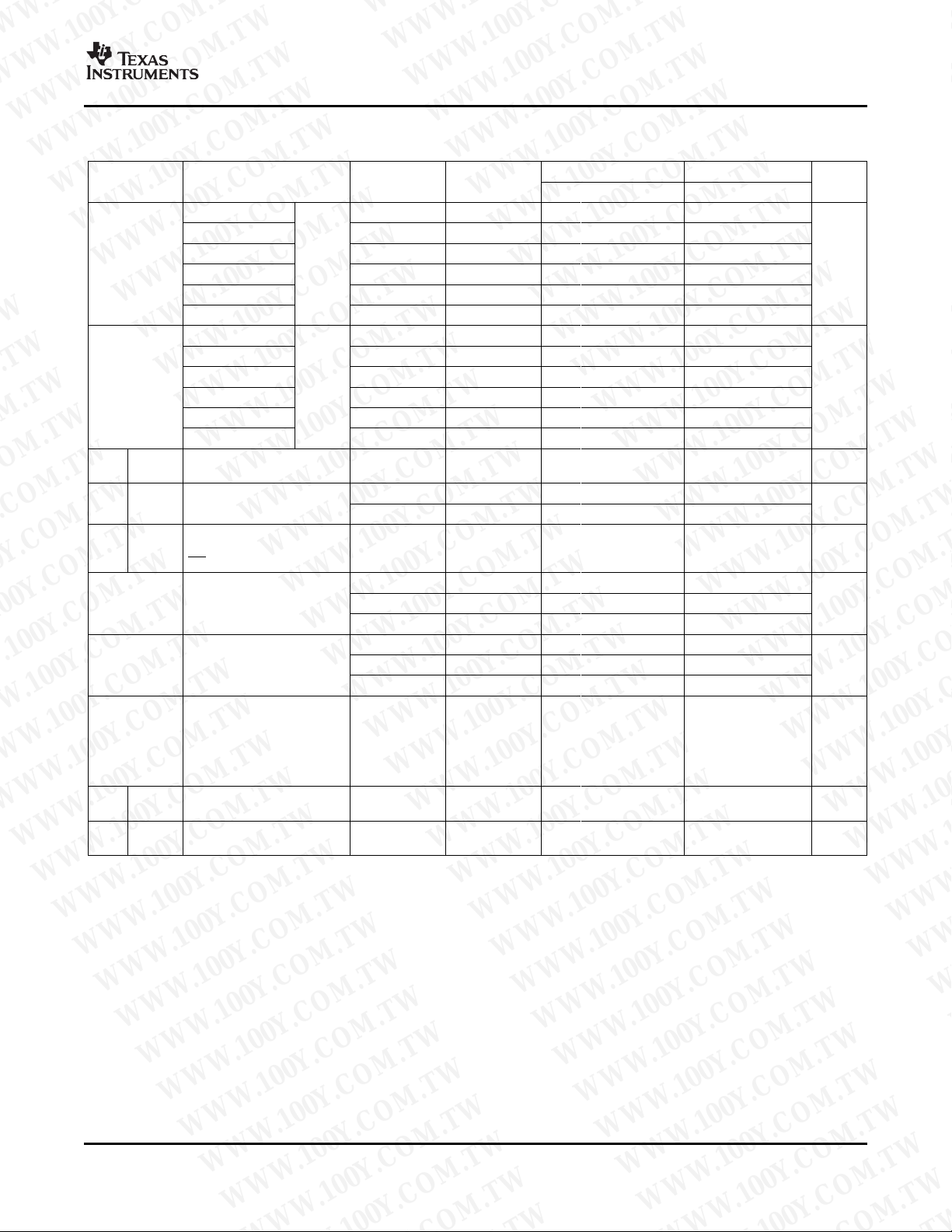
FUNCTION TABLE
(each 8-bit section)
INPUTS
OE DIR
L L B data to A bus
L H A data to B bus
H X All outputs Hi-Z
OPERATION
. The I
off
off
.
CCA
circuitry disables the outputs,
CC
through a pullup
LOGIC DIAGRAM (POSITIVE LOGIC)
WWW.100Y.COM.TW WWW.100Y.COM.TW WWW.100Y.COM.TW
WWW.100Y.COM.TW WWW.100Y.COM.TW WWW.100Y.COM.TW
WWW.100Y.COM.TW WWW.100Y.COM.TW WWW.100Y.COM.TW
WWW.100Y.COM.TW WWW.100Y.COM.TW WWW.100Y.COM.TW
WWW.100Y.COM.TW WWW.100Y.COM.TW WWW.100Y.COM.TW
WWW.100Y.COM.TW WWW.100Y.COM.TW WWW.100Y.COM.TW
WWW.100Y.COM.TW WWW.100Y.COM.TW WWW.100Y.COM.TW
WWW.100Y.COM.TW WWW.100Y.COM.TW WWW.100Y.COM.TW
WWW.100Y.COM.TW WWW.100Y.COM.TW WWW.100Y.COM.TW
2
WWW.100Y.COM.TW WWW.100Y.COM.TW WWW.100Y.COM.TW
Submit Documentation Feedback
WWW.100Y.COM.TW WWW.100Y.COM.TW WWW.100Y.COM.TW
Page 3
www.ti.com
SN74AVC8T245
8-BIT DUAL-SUPPLY BUS TRANSCEIVER
WITH CONFIGURABLE VOLTAGE TRANSLATION AND 3-STATE OUTPUTS
SCES517H – DECEMBER 2003 – REVISED FEBRUARY 2007
Absolute Maximum Ratings
over operating free-air temperature range (unless otherwise noted)
V
CCA
V
V
V
V
I
I
I
θ
T
(1) Stresses beyond those listed under "absolute maximum ratings" may cause permanent damage to the device. These are stress ratings
(2) The input voltage and output negative-voltage ratings may be exceeded if the input and output current ratings are observed.
(3) The output positive-voltage rating may be exceeded up to 4.6 V maximum if the output current rating is observed.
(4) The package thermal impedance is calculated in accordance with JESD 51-7.
Supply voltage range –0.5 4.6 V
CCB
Input voltage range
I
Voltage range applied to any output
O
in the high-impedance or power-off state
Voltage range applied to any output in the high or low state
O
Input clamp current VI< 0 –50 mA
IK
Output clamp current VO< 0 –50 mA
OK
Continuous output current ± 50 mA
O
Continuous current through V
Package thermal impedance
JA
Storage temperature range –65 150 ° C
stg
only, and functional operation of the device at these or any other conditions beyond those indicated under "recommended operating
conditions" is not implied. Exposure to absolute-maximum-rated conditions for extended periods may affect device reliability.
(2)
(1)
MIN MAX UNIT
I/O ports (A port) –0.5 4.6
I/O ports (B port) –0.5 4.6 V
Control inputs –0.5 4.6
(2)
(2) (3)
, V
CCA
(4)
, or GND ± 100 mA
CCB
A port –0.5 4.6
B port –0.5 4.6
A port –0.5 V
B port –0.5 V
DGV package 86
PW package 88 ° C/W
RHL package 43
+ 0.5
CCA
+ 0.5
CCB
V
V
WWW.100Y.COM.TW WWW.100Y.COM.TW WWW.100Y.COM.TW
WWW.100Y.COM.TW WWW.100Y.COM.TW WWW.100Y.COM.TW
WWW.100Y.COM.TW WWW.100Y.COM.TW WWW.100Y.COM.TW
WWW.100Y.COM.TW WWW.100Y.COM.TW WWW.100Y.COM.TW
WWW.100Y.COM.TW WWW.100Y.COM.TW WWW.100Y.COM.TW
WWW.100Y.COM.TW WWW.100Y.COM.TW WWW.100Y.COM.TW
WWW.100Y.COM.TW WWW.100Y.COM.TW WWW.100Y.COM.TW
WWW.100Y.COM.TW WWW.100Y.COM.TW WWW.100Y.COM.TW
WWW.100Y.COM.TW WWW.100Y.COM.TW WWW.100Y.COM.TW
WWW.100Y.COM.TW WWW.100Y.COM.TW WWW.100Y.COM.TW
Submit Documentation Feedback
3
WWW.100Y.COM.TW WWW.100Y.COM.TW WWW.100Y.COM.TW
Page 4
www.ti.com
SN74AVC8T245
8-BIT DUAL-SUPPLY BUS TRANSCEIVER
WITH CONFIGURABLE VOLTAGE TRANSLATION AND 3-STATE OUTPUTS
SCES517H – DECEMBER 2003 – REVISED FEBRUARY 2007
Recommended Operating Conditions
V
CCA
V
CCB
V
IH
V
IL
V
IH
V
IL
V
I
V
O
I
OH
I
OL
∆ t/ ∆ v Input transition rise or fall rate 5 ns/V
T
A
(1) V
(2) V
(3) All unused data inputs of the device must be held at V
Supply voltage 1.2 3.6 V
Supply voltage 1.2 3.6 V
High-level
input voltage
Low-level
input voltage
High-level DIR
input voltage (referenced to V
Low-level DIR
input voltage (referenced to V
Input voltage 0 3.6 V
Output voltage V
High-level output current 1.65 V to 1.95 V –8 mA
Low-level output current 1.65 V to 1.95 V 8 mA
Operating free-air temperature –40 85 ° C
is the V
CCI
is the V
CCO
Implications of Slow or Floating CMOS Inputs, literature number SCBA004.
associated with the input port.
CC
associated with the output port.
CC
Data inputs 1.95 V to 2.7 V 1.6 V
Data inputs 1.95 V to 2.7 V 0.7 V
Active state 0 V
3-state 0 3.6
(1) (2) (3)
V
CCI
1.2 V to 1.95 V V
2.7 V to 3.6 V 2
1.2 V to 1.95 V V
2.7 V to 3.6 V 0.8
1.2 V to 1.95 V V
1.95 V to 2.7 V 1.6 V
)
CCA
CCA
2.7 V to 3.6 V 2
1.2 V to 1.95 V V
1.95 V to 2.7 V 0.7 V
)
2.7 V to 3.6 V 0.8
or GND to ensure proper device operation. Refer to the TI application report,
CCI
V
CCO
1.2 V –3
1.4 V to 1.6 V –6
2.3 V to 2.7 V –9
3 V to 3.6 V –12
1.2 V 3
1.4 V to 1.6 V 6
2.3 V to 2.7 V 9
3 V to 3.6 V 12
MIN MAX UNIT
× 0.65
CCI
× 0.65
CCA
× 0.35
CCI
× 0.35
CCA
CCO
WWW.100Y.COM.TW WWW.100Y.COM.TW WWW.100Y.COM.TW
WWW.100Y.COM.TW WWW.100Y.COM.TW WWW.100Y.COM.TW
WWW.100Y.COM.TW WWW.100Y.COM.TW WWW.100Y.COM.TW
WWW.100Y.COM.TW WWW.100Y.COM.TW WWW.100Y.COM.TW
WWW.100Y.COM.TW WWW.100Y.COM.TW WWW.100Y.COM.TW
WWW.100Y.COM.TW WWW.100Y.COM.TW WWW.100Y.COM.TW
WWW.100Y.COM.TW WWW.100Y.COM.TW WWW.100Y.COM.TW
WWW.100Y.COM.TW WWW.100Y.COM.TW WWW.100Y.COM.TW
WWW.100Y.COM.TW WWW.100Y.COM.TW WWW.100Y.COM.TW
4
WWW.100Y.COM.TW WWW.100Y.COM.TW WWW.100Y.COM.TW
Submit Documentation Feedback
WWW.100Y.COM.TW WWW.100Y.COM.TW WWW.100Y.COM.TW
Page 5
www.ti.com
SN74AVC8T245
8-BIT DUAL-SUPPLY BUS TRANSCEIVER
WITH CONFIGURABLE VOLTAGE TRANSLATION AND 3-STATE OUTPUTS
SCES517H – DECEMBER 2003 – REVISED FEBRUARY 2007
Electrical Characteristics
(1) (2)
over recommended operating free-air temperature range (unless otherwise noted)
PARAMETER TEST CONDITIONS V
IOH= –100 µ A 1.2 V to 3.6 V 1.2 V to 3.6 V V
IOH= –3 mA 1.2 V 1.2 V 0.95
V
OH
V
OL
Control
I
I
inputs
A or B
I
off
port
A or B
(3)
I
OZ
port
I
CCA
I
CCB
I<Subscript>C
CA</Subscript
> +
I<Subscript>C
CB</Subscript
>
Control
C
i
inputs
A or B
C
WWW.100Y.COM.TW WWW.100Y.COM.TW WWW.100Y.COM.TW
WWW.100Y.COM.TW WWW.100Y.COM.TW WWW.100Y.COM.TW
io
port
(1) V
CCO
(2) V
CCI
(3) For I/O ports, the parameter IOZincludes the input leakage current.
IOH= –6 mA 1.4 V 1.4 V 1.05
IOH= –8 mA 1.65 V 1.65 V 1.2
IOH= –9 mA 2.3 V 2.3 V 1.75
IOH= –12 mA 3 V 3 V 2.3
IOL= 100 µ A 1.2 V to 3.6 V 1.2 V to 3.6 V 0.2
IOL= 3 mA 1.2 V 1.2 V 0.15
IOL= 6 mA 1.4 V 1.4 V 0.35
IOL= 8 mA 1.65 V 1.65 V 0.45
IOL= 9 mA 2.3 V 2.3 V 0.55
IOL= 12 mA 3 V 3 V 0.7
VI= V
VIor VO= 0 to 3.6 V µ A
VO= V
VI= V
OE = V
VI= V
VI= V
VI= V
VI= 3.3 V or GND 3.3 V 3.3 V 3.5 4.5 pF
VO= 3.3 V or GND 3.3 V 3.3 V 6 7 pF
is the V
is the V
CC
CC
or GND 1.2 V to 3.6 V 1.2 V to 3.6 V ± 0.025 ± 0.25 ± 1 µ A
CCA
or GND,
CCO
or GND, 3.6 V 3.6 V ± 0.5 ± 2.5 ± 5 µ A
CCI
IH
or GND, IO= 0 0 V 3.6 V –2 µ A
CCI
or GND, IO= 0 0 V 3.6 V 15 µ A
CCI
or GND, IO= 0 1.2 V to 3.6 V 1.2 V to 3.6 V 25 µ A
CCI
associated with the output port.
associated with the input port.
VI= V
VI= V
IH
IL
CCA
0 V 0 V to 3.6 V ± 0.1 ± 1 ± 5
0 V to 3.6 V 0 V ± 0.1 ± 1 ± 5
1.2 V to 3.6 V 1.2 V to 3.6 V 15
3.6 V 0 V 15
1.2 V to 3.6 V 1.2 V to 3.6 V 15
3.6 V 0 V –2
V
CCB
TA= 25 ° C –40 ° C to 85 ° C
MIN TYP MAX MIN MAX
– 0.2
CCO
UNIT
V
V
WWW.100Y.COM.TW WWW.100Y.COM.TW WWW.100Y.COM.TW
WWW.100Y.COM.TW WWW.100Y.COM.TW WWW.100Y.COM.TW
WWW.100Y.COM.TW WWW.100Y.COM.TW WWW.100Y.COM.TW
WWW.100Y.COM.TW WWW.100Y.COM.TW WWW.100Y.COM.TW
WWW.100Y.COM.TW WWW.100Y.COM.TW WWW.100Y.COM.TW
WWW.100Y.COM.TW WWW.100Y.COM.TW WWW.100Y.COM.TW
WWW.100Y.COM.TW WWW.100Y.COM.TW WWW.100Y.COM.TW
WWW.100Y.COM.TW WWW.100Y.COM.TW WWW.100Y.COM.TW
Submit Documentation Feedback
5
WWW.100Y.COM.TW WWW.100Y.COM.TW WWW.100Y.COM.TW
Page 6
www.ti.com
SN74AVC8T245
8-BIT DUAL-SUPPLY BUS TRANSCEIVER
WITH CONFIGURABLE VOLTAGE TRANSLATION AND 3-STATE OUTPUTS
SCES517H – DECEMBER 2003 – REVISED FEBRUARY 2007
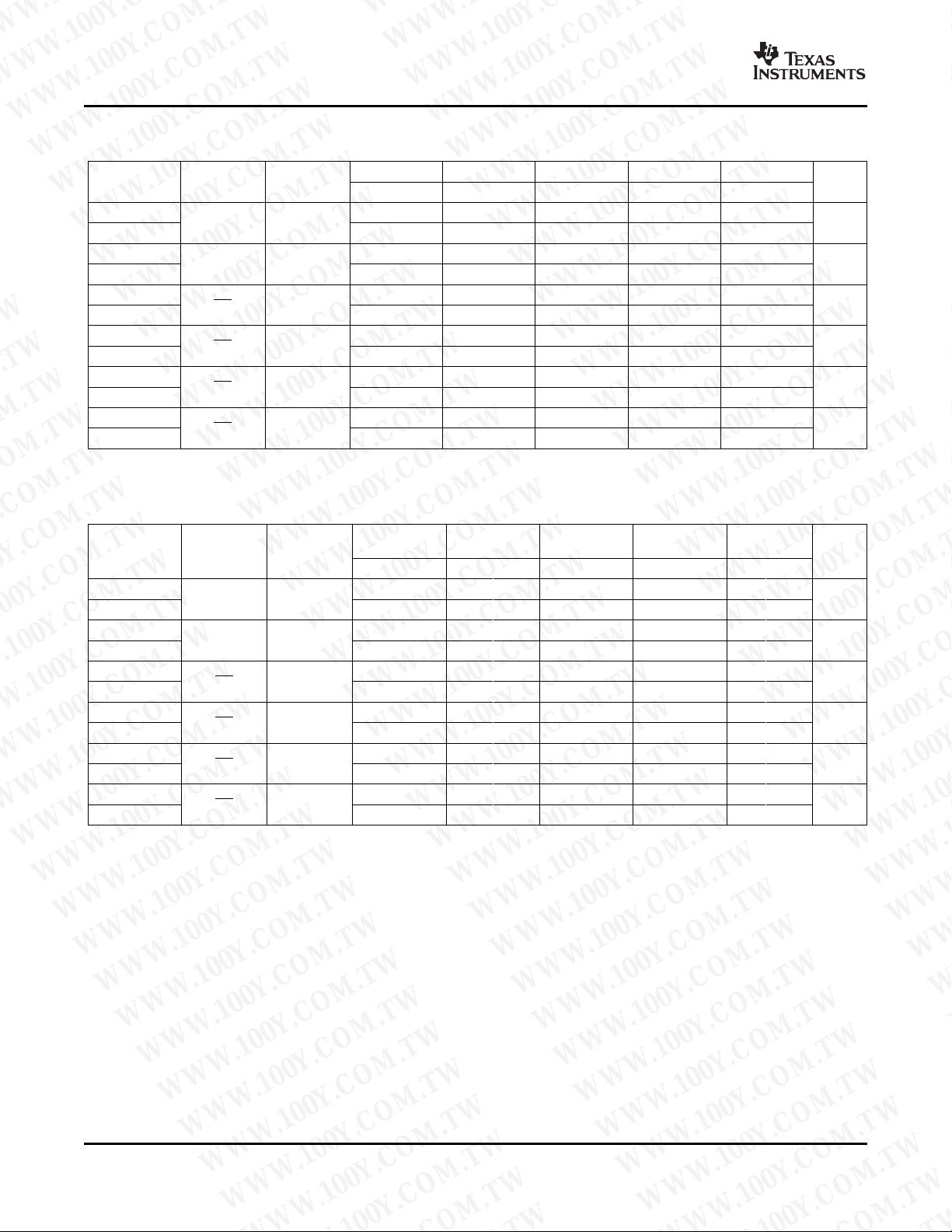
Switching Characteristics
over recommended operating free-air temperature range, V
V
= 1.2 V V
PARAMETER UNIT
t
PLH
t
PHL
t
PLH
t
PHL
t
PZH
t
PZL
t
PZH
t
PZL
t
PHZ
t
PLZ
t
PHZ
t
PLZ
FROM TO
(INPUT) (OUTPUT)
A B ns
B A ns
OE A ns
OE B ns
OE A ns
OE B ns
CCB
TYP TYP TYP TYP TYP
3.1 2.6 2.5 3 3.5
3.1 2.6 2.5 3 3.5
3.1 2.7 2.5 2.4 2.3
3.1 2.7 2.5 2.4 2.3
5.3 5.3 5.3 5.3 5.3
5.3 5.3 5.3 5.3 5.3
5.1 4 3.5 3.2 3.1
5.1 4 3.5 3.2 3.1
4.8 4.8 4.8 4.8 4.8
4.8 4.8 4.8 4.8 4.8
4.7 4 4.1 4.3 5.1
4.7 4 4.1 4.3 5.1
= 1.2 V (see Figure 10 )
CCA
= 1.5 V V
CCB
CCB
= 1.8 V V
CCB
= 2.5 V V
CCB
= 3.3 V
Switching Characteristics
over recommended operating free-air temperature range, V
V
= 1.2 V
PARAMETER UNIT
t
PLH
t
PHL
t
PLH
t
PHL
t
PZH
t
PZL
t
PZH
t
PZL
t
PHZ
t
PLZ
t
PHZ
t
PLZ
FROM TO
(INPUT) (OUTPUT)
A B ns
B A ns
OE A ns
OE B ns
OE A ns
OE B ns
CCB
TYP MIN MAX MIN MAX MIN MAX MIN MAX
2.7 0.5 5.4 0.5 4.6 0.5 4.9 0.5 6.8
2.7 0.5 5.4 0.5 4.6 0.5 4.9 0.5 6.8
2.6 0.5 5.4 0.5 5.1 0.5 4.7 0.5 4.5
2.6 0.5 5.4 0.5 5.1 0.5 4.7 0.5 4.5
3.7 1.1 8.7 1.1 8.7 1.1 8.7 1.1 8.7
3.7 1.1 8.7 1.1 8.7 1.1 8.7 1.1 8.7
4.8 1.1 7.6 1.1 7.1 1 5.6 1 5.2
4.8 1.1 7.6 1.1 7.1 1 5.6 1 5.2
3.1 0.5 8.6 0.5 8.6 0.5 8.6 0.5 8.6
3.1 0.5 8.6 0.5 8.6 0.5 8.6 0.5 8.6
4.1 0.5 8.4 0.5 7.6 0.5 7.2 0.5 7.8
4.1 0.5 8.4 0.5 7.6 0.5 7.2 0.5 7.8
= 1.5 V ± 0.1 V (see Figure 10 )
CCA
V
= 1.5 V V
CCB
± 0.1 V ± 0.15 V ± 0.2 V ± 0.3 V
CCB
= 1.8 V V
CCB
= 2.5 V V
= 3.3 V
CCB
WWW.100Y.COM.TW WWW.100Y.COM.TW WWW.100Y.COM.TW
WWW.100Y.COM.TW WWW.100Y.COM.TW WWW.100Y.COM.TW
WWW.100Y.COM.TW WWW.100Y.COM.TW WWW.100Y.COM.TW
WWW.100Y.COM.TW WWW.100Y.COM.TW WWW.100Y.COM.TW
WWW.100Y.COM.TW WWW.100Y.COM.TW WWW.100Y.COM.TW
WWW.100Y.COM.TW WWW.100Y.COM.TW WWW.100Y.COM.TW
WWW.100Y.COM.TW WWW.100Y.COM.TW WWW.100Y.COM.TW
WWW.100Y.COM.TW WWW.100Y.COM.TW WWW.100Y.COM.TW
WWW.100Y.COM.TW WWW.100Y.COM.TW WWW.100Y.COM.TW
6
WWW.100Y.COM.TW WWW.100Y.COM.TW WWW.100Y.COM.TW
Submit Documentation Feedback
WWW.100Y.COM.TW WWW.100Y.COM.TW WWW.100Y.COM.TW
Page 7
www.ti.com
SN74AVC8T245
8-BIT DUAL-SUPPLY BUS TRANSCEIVER
WITH CONFIGURABLE VOLTAGE TRANSLATION AND 3-STATE OUTPUTS
SCES517H – DECEMBER 2003 – REVISED FEBRUARY 2007
Switching Characteristics
over recommended operating free-air temperature range, V
V
= 1.2 V
PARAMETER UNIT
t
PLH
t
PHL
t
PLH
t
PHL
t
PZH
t
PZL
t
PZH
t
PZL
t
PHZ
t
PLZ
t
PHZ
t
PLZ
FROM TO
(INPUT) (OUTPUT)
A B ns
B A ns
OE A ns
OE B ns
OE A ns
OE B ns
CCB
TYP MIN MAX MIN MAX MIN MAX MIN MAX
2.5 0.5 5.1 0.5 4.4 0.5 4 0.5 3.9
2.5 0.5 5.1 0.5 4.4 0.5 4 0.5 3.9
2.5 0.5 4.6 0.5 4.4 0.5 3.9 0.5 3.7
2.5 0.5 4.6 0.5 4.4 0.5 3.9 0.5 3.7
3 1 6.8 1 6.8 1 6.8 1 6.8
3 1 6.8 1 6.8 1 6.8 1 6.8
4.6 1.1 8.2 1 6.7 0.5 5.1 0.5 4.5
4.6 1.1 8.2 1 6.7 0.5 5.1 0.5 4.5
2.8 0.5 7.1 0.5 7.1 0.5 7.1 0.5 7.1
2.8 0.5 7.1 0.5 7.1 0.5 7.1 0.5 7.1
3.9 0.5 7.8 0.5 6.9 0.5 6 0.5 5.8
3.9 0.5 7.8 0.5 6.9 0.5 6 0.5 5.8
= 1.8 V ± 0.15 V (see Figure 10 )
CCA
V
= 1.5 V V
CCB
± 0.1 V ± 0.15 V ± 0.2 V ± 0.3 V
CCB
= 1.8 V V
CCB
= 2.5 V V
= 3.3 V
CCB
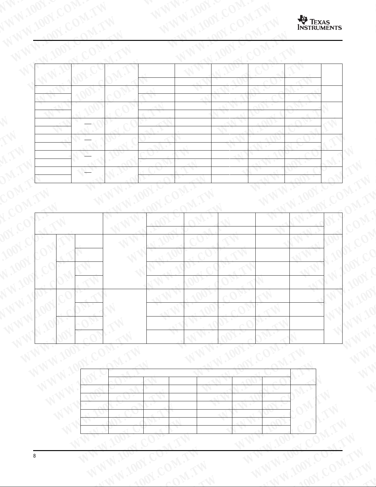
Switching Characteristics
over recommended operating free-air temperature range, V
V
= 1.2 V
PARAMETER UNIT
t
PLH
t
PHL
t
PLH
t
PHL
t
PZH
t
PZL
t
PZH
t
PZL
t
PHZ
t
PLZ
t
PHZ
t
WWW.100Y.COM.TW WWW.100Y.COM.TW WWW.100Y.COM.TW
PLZ
FROM TO
(INPUT) (OUTPUT)
A B ns
B A ns
OE A ns
OE B ns
OE A ns
OE B ns
CCB
TYP MIN MAX MIN MAX MIN MAX MIN MAX
2.4 0.5 4.7 0.5 3.9 0.5 3.1 0.5 2.8
2.4 0.5 4.7 0.5 3.9 0.5 3.1 0.5 2.8
3 0.5 4.9 0.5 4 0.5 3.1 0.5 2.9
3 0.5 4.9 0.5 4 0.5 3.1 0.5 2.9
2.2 0.5 4.8 0.5 4.8 0.5 4.8 0.5 4.8
2.2 0.5 4.8 0.5 4.8 0.5 4.8 0.5 4.8
4.5 1.1 7.9 0.5 6.4 0.5 4.6 0.5 4
4.5 1.1 7.9 0.5 6.4 0.5 4.6 0.5 4
1.8 0.5 5.1 0.5 5.1 0.5 5.1 0.5 5.1
1.8 0.5 5.1 0.5 5.1 0.5 5.1 0.5 5.1
3.6 0.5 7.1 0.5 6.3 0.5 5.1 0.5 3.9
3.6 0.5 7.1 0.5 6.3 0.5 5.1 0.5 3.9
= 2.5 V ± 0.2 V (see Figure 10 )
CCA
V
= 1.5 V V
CCB
± 0.1 V ± 0.15 V ± 0.2 V ± 0.3 V
CCB
= 1.8 V V
CCB
= 2.5 V V
= 3.3 V
CCB
WWW.100Y.COM.TW WWW.100Y.COM.TW WWW.100Y.COM.TW
WWW.100Y.COM.TW WWW.100Y.COM.TW WWW.100Y.COM.TW
WWW.100Y.COM.TW WWW.100Y.COM.TW WWW.100Y.COM.TW
WWW.100Y.COM.TW WWW.100Y.COM.TW WWW.100Y.COM.TW
WWW.100Y.COM.TW WWW.100Y.COM.TW WWW.100Y.COM.TW
WWW.100Y.COM.TW WWW.100Y.COM.TW WWW.100Y.COM.TW
WWW.100Y.COM.TW WWW.100Y.COM.TW WWW.100Y.COM.TW
WWW.100Y.COM.TW WWW.100Y.COM.TW WWW.100Y.COM.TW
WWW.100Y.COM.TW WWW.100Y.COM.TW WWW.100Y.COM.TW
Submit Documentation Feedback
7
WWW.100Y.COM.TW WWW.100Y.COM.TW WWW.100Y.COM.TW
Page 8
www.ti.com
SN74AVC8T245
8-BIT DUAL-SUPPLY BUS TRANSCEIVER
WITH CONFIGURABLE VOLTAGE TRANSLATION AND 3-STATE OUTPUTS
SCES517H – DECEMBER 2003 – REVISED FEBRUARY 2007
Switching Characteristics
over recommended operating free-air temperature range, V
V
= 1.2 V
PARAMETER UNIT
t
PLH
t
PHL
t
PLH
t
PHL
t
PZH
t
PZL
t
PZH
t
PZL
t
PHZ
t
PLZ
t
PHZ
t
PLZ
FROM TO
(INPUT) (OUTPUT)
A B ns
B A ns
OE A ns
OE B ns
OE A ns
OE B ns
CCB
TYP MIN MAX MIN MAX MIN MAX MIN MAX
2.3 0.5 4.5 0.5 3.7 0.5 2.9 0.5 2.5
2.3 0.5 4.5 0.5 3.3 0.5 2.9 0.5 2.5
3.5 0.5 6.8 0.5 3.9 0.5 2.8 0.5 2.5
3.5 0.5 6.8 0.5 3.9 0.5 2.8 0.5 2.5
2 0.5 4 0.5 4 0.5 4 0.5 4
2 0.5 4 0.5 4 0.5 4 0.5 4
4.5 1.1 7.8 0.5 6.2 0.5 4.5 0.5 3.9
4.5 1.1 7.8 0.5 6.2 0.5 4.5 0.5 3.9
1.7 0.5 4 0.5 4 0.5 4 0.5 4
1.7 0.5 4 0.5 4 0.5 4 0.5 4
3.4 0.5 6.9 0.5 6 0.5 4.8 0.5 4.2
3.4 0.5 6.9 0.5 6 0.5 4.8 0.5 4.2
= 3.3 V ± 0.3 V (see Figure 10 )
CCA
V
= 1.5 V V
CCB
± 0.1 V ± 0.15 V ± 0.2 V ± 0.3 V
CCB
= 1.8 V V
CCB
= 2.5 V V
CCB
= 3.3 V
Operating Characteristics
TA= 25 ° C
V
= V
PARAMETER UNIT
Outputs
enabled
A to B
Outputs
B to A
A to B
B to A
disabled
Outputs
enabled
Outputs
disabled
Outputs
enabled
Outputs
disabled
Outputs
enabled
Outputs
disabled
(1)
C
pdA
(1)
C
pdB
WWW.100Y.COM.TW WWW.100Y.COM.TW WWW.100Y.COM.TW
WWW.100Y.COM.TW WWW.100Y.COM.TW WWW.100Y.COM.TW
(1) Power dissipation capacitance per transceiver
WWW.100Y.COM.TW WWW.100Y.COM.TW WWW.100Y.COM.TW
WWW.100Y.COM.TW WWW.100Y.COM.TW WWW.100Y.COM.TW
WWW.100Y.COM.TW WWW.100Y.COM.TW WWW.100Y.COM.TW
WWW.100Y.COM.TW WWW.100Y.COM.TW WWW.100Y.COM.TW
WWW.100Y.COM.TW WWW.100Y.COM.TW WWW.100Y.COM.TW
WWW.100Y.COM.TW WWW.100Y.COM.TW WWW.100Y.COM.TW
V
CCB
0 V 0 <0.5 <0.5 <0.5 <0.5 <0.5
1.2 V <0.5 <1 <1 <1 <1 1
1.5 V <0.5 <1 <1 <1 <1 1
1.8 V <0.5 <1 <1 <1 <1 <1
2.5 V <0.5 1 <1 <1 <1 <1
3.3 V <0.5 1 <1 <1 <1 <1
TEST
CONDITIONS
CL= 0,
f = 10 MHz, pF
tr= tf= 1 ns
CL= 0,
f = 10 MHz, pF
tr= tf= 1 ns
Table 1. Typical Total Static Power Consumption (I
0 V 1.2 V 1.5 V 1.8 V 2.5 V 3.3 V
CCA
V
= 1.2 V V
CCB
TYP TYP TYP TYP TYP
1 1 1 1 1
1 1 1 1 1
12 12 12 13 14
1 1 1 1 1
12 12 12 13 14
1 1 1 1 1
1 1 1 1 1
1 1 1 1 1
CCB
V
= V
CCA
= 1.5 V V
CCA
CCB
= V
CCA
= 1.8 V V
= V
CCA
= 2.5 V V
CCB
+ I
CCA
)
CCB
=
CCA
= 3.3 V
CCB
UNIT
µ A
WWW.100Y.COM.TW WWW.100Y.COM.TW WWW.100Y.COM.TW
8
Submit Documentation Feedback
WWW.100Y.COM.TW WWW.100Y.COM.TW WWW.100Y.COM.TW
WWW.100Y.COM.TW WWW.100Y.COM.TW WWW.100Y.COM.TW
Page 9

www.ti.com
0
1
2
3
4
5
6
0 10 20 30 40 50
t
PD
− ns
C
L
− pF
60
V
CCB
= 1.8 V
V
CCB
= 2.5 V
V
CCB
= 3.3 V
V
CCB
= 1.5 V
V
CCB
= 1.2 V
C
L
− pF
0
1
2
3
4
5
6
V
CCB
= 1.8 V
V
CCB
= 2.5 V
V
CCB
= 3.3 V
V
CCB
= 1.5 V
V
CCB
= 1.2 V
0
10 20 30 40 50 60
t
PLH
− ns
0
1
2
3
4
5
6
0
10 20 30 40 50 60
t
PHL
− ns
C
L
− pF
V
CCB
= 1.8 V
V
CCB
= 2.5 V
V
CCB
= 3.3 V
V
CCB
= 1.5 V
V
CCB
= 1.2 V
WITH CONFIGURABLE VOLTAGE TRANSLATION AND 3-STATE OUTPUTS
Typical Propagation Delay (A to B) vs Load Capacitance
T
= 25 ° C, V
A
= 1.2 V
CCA
SN74AVC8T245
8-BIT DUAL-SUPPLY BUS TRANSCEIVER
SCES517H – DECEMBER 2003 – REVISED FEBRUARY 2007
TYPICAL CHARACTERISTICS
Figure 1.
Typical Propagation Delay (A to B) vs Load Capacitance
T
= 25 ° C, V
A
= 1.5 V
CCA
WWW.100Y.COM.TW WWW.100Y.COM.TW WWW.100Y.COM.TW
WWW.100Y.COM.TW WWW.100Y.COM.TW WWW.100Y.COM.TW
WWW.100Y.COM.TW WWW.100Y.COM.TW WWW.100Y.COM.TW
WWW.100Y.COM.TW WWW.100Y.COM.TW WWW.100Y.COM.TW
WWW.100Y.COM.TW WWW.100Y.COM.TW WWW.100Y.COM.TW
Figure 2. Figure 3.
WWW.100Y.COM.TW WWW.100Y.COM.TW WWW.100Y.COM.TW
WWW.100Y.COM.TW WWW.100Y.COM.TW WWW.100Y.COM.TW
WWW.100Y.COM.TW WWW.100Y.COM.TW WWW.100Y.COM.TW
WWW.100Y.COM.TW WWW.100Y.COM.TW WWW.100Y.COM.TW
WWW.100Y.COM.TW WWW.100Y.COM.TW WWW.100Y.COM.TW
WWW.100Y.COM.TW WWW.100Y.COM.TW WWW.100Y.COM.TW
Submit Documentation Feedback
9
Page 10

www.ti.com
CL − pF
t
PLH
− ns
0
10 20 30 40 50 60
0
1
2
3
4
5
6
V
CCB
= 1.8 V
V
CCB
= 2.5 V
V
CCB
= 3.3 V
V
CCB
= 1.5 V
V
CCB
= 1.2 V
0
1
2
3
4
5
6
0
10 20 30 40 50 60
V
CCB
= 1.8 V
V
CCB
= 2.5 V
V
CCB
= 3.3 V
V
CCB
= 1.5 V
V
CCB
= 1.2 V
t
PHL
− ns
CL − pF
CL − pF
t
PLH
− ns
V
CCB
= 1.8 V
V
CCB
= 2.5 V
V
CCB
= 3.3 V
V
CCB
= 1.5 V
V
CCB
= 1.2 V
0
1
2
3
4
5
6
0
10 20 30 40 50 60
0
1
2
3
4
5
6
0
10 20 30 40 50 60
V
CCB
= 1.8 V
V
CCB
= 2.5 V
V
CCB
= 3.3 V
V
CCB
= 1.5 V
V
CCB
= 1.2 V
CL − pF
t
PHL
− ns
SN74AVC8T245
8-BIT DUAL-SUPPLY BUS TRANSCEIVER
WITH CONFIGURABLE VOLTAGE TRANSLATION AND 3-STATE OUTPUTS
SCES517H – DECEMBER 2003 – REVISED FEBRUARY 2007
TYPICAL CHARACTERISTICS (continued)
Typical Propagation Delay (A to B) vs Load Capacitance
T
= 25 ° C, V
A
= 1.8 V
CCA
Figure 4. Figure 5.
Typical Propagation Delay (A to B) vs Load Capacitance
T
= 25 ° C, V
A
= 2.5 V
CCA
WWW.100Y.COM.TW WWW.100Y.COM.TW WWW.100Y.COM.TW
WWW.100Y.COM.TW WWW.100Y.COM.TW WWW.100Y.COM.TW
WWW.100Y.COM.TW WWW.100Y.COM.TW WWW.100Y.COM.TW
WWW.100Y.COM.TW WWW.100Y.COM.TW WWW.100Y.COM.TW
WWW.100Y.COM.TW WWW.100Y.COM.TW WWW.100Y.COM.TW
Figure 6. Figure 7.
WWW.100Y.COM.TW WWW.100Y.COM.TW WWW.100Y.COM.TW
WWW.100Y.COM.TW WWW.100Y.COM.TW WWW.100Y.COM.TW
WWW.100Y.COM.TW WWW.100Y.COM.TW WWW.100Y.COM.TW
WWW.100Y.COM.TW WWW.100Y.COM.TW WWW.100Y.COM.TW
10
WWW.100Y.COM.TW WWW.100Y.COM.TW WWW.100Y.COM.TW
WWW.100Y.COM.TW WWW.100Y.COM.TW WWW.100Y.COM.TW
Submit Documentation Feedback
Page 11

www.ti.com
t
PLH
− ns
0
1
2
3
4
5
6
V
CCB
= 1.8 V
V
CCB
= 2.5 V
V
CCB
= 3.3 V
V
CCB
= 1.5 V
V
CCB
= 1.2 V
CL − pF
0
10 20 30 40 50 60
0
1
2
3
4
5
6
0
10 20 30 40 50 60
V
CCB
= 1.8 V
V
CCB
= 2.5 V
V
CCB
= 3.3 V
V
CCB
= 1.5 V
V
CCB
= 1.2 V
CL − pF
t
PHL
− ns
WITH CONFIGURABLE VOLTAGE TRANSLATION AND 3-STATE OUTPUTS
TYPICAL CHARACTERISTICS (continued)
Typical Propagation Delay (A to B) vs Load Capacitance
T
= 25 ° C, V
A
= 3.3 V
CCA
SN74AVC8T245
8-BIT DUAL-SUPPLY BUS TRANSCEIVER
SCES517H – DECEMBER 2003 – REVISED FEBRUARY 2007
Figure 8. Figure 9.
WWW.100Y.COM.TW WWW.100Y.COM.TW WWW.100Y.COM.TW
WWW.100Y.COM.TW WWW.100Y.COM.TW WWW.100Y.COM.TW
WWW.100Y.COM.TW WWW.100Y.COM.TW WWW.100Y.COM.TW
WWW.100Y.COM.TW WWW.100Y.COM.TW WWW.100Y.COM.TW
WWW.100Y.COM.TW WWW.100Y.COM.TW WWW.100Y.COM.TW
WWW.100Y.COM.TW WWW.100Y.COM.TW WWW.100Y.COM.TW
WWW.100Y.COM.TW WWW.100Y.COM.TW WWW.100Y.COM.TW
WWW.100Y.COM.TW WWW.100Y.COM.TW WWW.100Y.COM.TW
WWW.100Y.COM.TW WWW.100Y.COM.TW WWW.100Y.COM.TW
WWW.100Y.COM.TW WWW.100Y.COM.TW WWW.100Y.COM.TW
WWW.100Y.COM.TW WWW.100Y.COM.TW WWW.100Y.COM.TW
Submit Documentation Feedback
11
Page 12

www.ti.com
V
OH
V
OL
From Output
Under Test
C
L
(see Note A)
LOAD CIRCUIT
S1
2 × V
CCO
Open
GND
R
L
R
L
t
PLH
t
PHL
Output
Control
(low-level
enabling)
Output
Waveform 1
S1 at 2 × V
CCO
(see Note B)
Output
Waveform 2
S1 at GND
(see Note B)
t
PZL
t
PZH
t
PLZ
t
PHZ
V
CCA
/2 V
CCA
/2
V
CCI
/2 V
CCI
/2
V
CCI
0 V
V
CCO
/2 V
CCO
/2
V
OH
V
OL
0 V
V
CCO
/2
VOL + V
TP
V
CCO
/2
VOH − V
TP
0 V
V
CCI
0 V
V
CCI
/2 V
CCI
/2
t
w
Input
V
CCA
V
CCO
VOLTAGE WAVEFORMS
PROPAGATION DELAY TIMES
VOLTAGE WAVEFORMS
PULSE DURATION
VOLTAGE WAVEFORMS
ENABLE AND DISABLE TIMES
Output
Input
t
pd
t
PLZ/tPZL
t
PHZ
/t
PZH
Open
2 × V
CCO
GND
TEST S1
NOTES: A. C
L
includes probe and jig capacitance.
B. Waveform 1 is for an output with internal conditions such that the output is low, except when disabled by the output control.
Waveform2 is for an output with internal conditions such that the output is high, except when disabled by the output control.
C.All input pulses are supplied by generators having the following characteristics: PRRv10 MHz, ZO = 50 Ω, dv/dt ≥ 1 V/ns.
D.The outputs are measured one at a time, with one transition per measurement.
E. t
PLZ
and t
PHZ
are the same as t
dis
.
F. t
PZL
and t
PZH
are the same as ten.
G. t
PLH
and t
PHL
are the same as tpd.
H. V
CCI
is the VCC associated with the input port.
I. V
CCO
is the VCC associated with the output port.
1.2 V
1.5 V ± 0.1 V
1.8 V ± 0.15 V
2.5 V ± 0.2 V
3.3 V ± 0.3 V
2 kΩ
2 kΩ
2 kΩ
2 kΩ
2 kΩ
V
CCO
R
L
0.1 V
0.1 V
0.15 V
0.15 V
0.3 V
V
TP
C
L
15 pF
15 pF
15 pF
15 pF
15 pF
SN74AVC8T245
8-BIT DUAL-SUPPLY BUS TRANSCEIVER
WITH CONFIGURABLE VOLTAGE TRANSLATION AND 3-STATE OUTPUTS
SCES517H – DECEMBER 2003 – REVISED FEBRUARY 2007
PARAMETER MEASUREMENT INFORMATION
WWW.100Y.COM.TW WWW.100Y.COM.TW WWW.100Y.COM.TW
WWW.100Y.COM.TW WWW.100Y.COM.TW WWW.100Y.COM.TW
WWW.100Y.COM.TW WWW.100Y.COM.TW WWW.100Y.COM.TW
WWW.100Y.COM.TW WWW.100Y.COM.TW WWW.100Y.COM.TW
12
WWW.100Y.COM.TW WWW.100Y.COM.TW WWW.100Y.COM.TW
WWW.100Y.COM.TW WWW.100Y.COM.TW WWW.100Y.COM.TW
WWW.100Y.COM.TW WWW.100Y.COM.TW WWW.100Y.COM.TW
WWW.100Y.COM.TW WWW.100Y.COM.TW WWW.100Y.COM.TW
WWW.100Y.COM.TW WWW.100Y.COM.TW WWW.100Y.COM.TW
WWW.100Y.COM.TW WWW.100Y.COM.TW WWW.100Y.COM.TW
WWW.100Y.COM.TW WWW.100Y.COM.TW WWW.100Y.COM.TW
Figure 10. Load Circuit and Voltage Waveforms
Submit Documentation Feedback
Page 13

PACKAGE OPTION ADDENDUM
www.ti.com 26-Mar-2010
PACKAGING INFORMATION
Orderable Device Status
74AVC8T245DGVRE4 ACTIVE TVSOP DGV 24 2000 Green (RoHS &
74AVC8T245DGVRG4 ACTIVE TVSOP DGV 24 2000 Green (RoHS &
74AVC8T245RHLRG4 ACTIVE QFN RHL 24 1000 Green (RoHS &
SN74AVC8T245DGVR ACTIVE TVSOP DGV 24 2000 Green (RoHS &
SN74AVC8T245PW ACTIVE TSSOP PW 24 60 Green (RoHS &
SN74AVC8T245PWE4 ACTIVE TSSOP PW 24 60 Green (RoHS &
SN74AVC8T245PWG4 ACTIVE TSSOP PW 24 60 Green (RoHS &
SN74AVC8T245PWR ACTIVE TSSOP PW 24 2000 Green (RoHS &
SN74AVC8T245PWRE4 ACTIVE TSSOP PW 24 2000 Green (RoHS &
SN74AVC8T245PWRG4 ACTIVE TSSOP PW 24 2000 Green (RoHS &
SN74AVC8T245RHLR ACTIVE QFN RHL 24 1000 Green (RoHS &
(1)
The marketing status values are defined as follows:
ACTIVE: Product device recommended for new designs.
LIFEBUY: TI has announced that the device will be discontinued, and a lifetime-buy period is in effect.
NRND: Not recommended for new designs. Device is in production to support existing customers, but TI does not recommend using this part in
a new design.
PREVIEW: Device has been announced but is not in production. Samples may or may not be available.
OBSOLETE: TI has discontinued the production of the device.
(1)
Package
Type
Package
Drawing
Pins Package
Qty
Eco Plan
no Sb/Br)
no Sb/Br)
no Sb/Br)
no Sb/Br)
no Sb/Br)
no Sb/Br)
no Sb/Br)
no Sb/Br)
no Sb/Br)
no Sb/Br)
no Sb/Br)
(2)
Lead/Ball Finish MSL Peak Temp
CU NIPDAU Level-1-260C-UNLIM
CU NIPDAU Level-1-260C-UNLIM
CU NIPDAU Level-2-260C-1 YEAR
CU NIPDAU Level-1-260C-UNLIM
CU NIPDAU Level-1-260C-UNLIM
CU NIPDAU Level-1-260C-UNLIM
CU NIPDAU Level-1-260C-UNLIM
CU NIPDAU Level-1-260C-UNLIM
CU NIPDAU Level-1-260C-UNLIM
CU NIPDAU Level-1-260C-UNLIM
CU NIPDAU Level-2-260C-1 YEAR
(3)
(2)
Eco Plan - The planned eco-friendly classification: Pb-Free (RoHS), Pb-Free (RoHS Exempt), or Green (RoHS & no Sb/Br) - please check
http://www.ti.com/productcontent for the latest availability information and additional product content details.
TBD: The Pb-Free/Green conversion plan has not been defined.
Pb-Free (RoHS): TI's terms "Lead-Free" or "Pb-Free" mean semiconductor products that are compatible with the current RoHS requirements
for all 6 substances, including the requirement that lead not exceed 0.1% by weight in homogeneous materials. Where designed to be soldered
at high temperatures, TI Pb-Free products are suitable for use in specified lead-free processes.
Pb-Free (RoHS Exempt): This component has a RoHS exemption for either 1) lead-based flip-chip solder bumps used between the die and
package, or 2) lead-based die adhesive used between the die and leadframe. The component is otherwise considered Pb-Free (RoHS
WWW.100Y.COM.TW WWW.100Y.COM.TW WWW.100Y.COM.TW
WWW.100Y.COM.TW WWW.100Y.COM.TW WWW.100Y.COM.TW
compatible) as defined above.
Green (RoHS & no Sb/Br): TI defines "Green" to mean Pb-Free (RoHS compatible), and free of Bromine (Br) and Antimony (Sb) based flame
retardants (Br or Sb do not exceed 0.1% by weight in homogeneous material)
(3)
WWW.100Y.COM.TW WWW.100Y.COM.TW WWW.100Y.COM.TW
MSL, Peak Temp. -- The Moisture Sensitivity Level rating according to the JEDEC industry standard classifications, and peak solder
temperature.
WWW.100Y.COM.TW WWW.100Y.COM.TW WWW.100Y.COM.TW
Important Information and Disclaimer:The information provided on this page represents TI's knowledge and belief as of the date that it is
provided. TI bases its knowledge and belief on information provided by third parties, and makes no representation or warranty as to the
accuracy of such information. Efforts are underway to better integrate information from third parties. TI has taken and continues to take
WWW.100Y.COM.TW WWW.100Y.COM.TW WWW.100Y.COM.TW
reasonable steps to provide representative and accurate information but may not have conducted destructive testing or chemical analysis on
incoming materials and chemicals. TI and TI suppliers consider certain information to be proprietary, and thus CAS numbers and other limited
information may not be available for release.
WWW.100Y.COM.TW WWW.100Y.COM.TW WWW.100Y.COM.TW
In no event shall TI's liability arising out of such information exceed the total purchase price of the TI part(s) at issue in this document sold by TI
WWW.100Y.COM.TW WWW.100Y.COM.TW WWW.100Y.COM.TW
WWW.100Y.COM.TW WWW.100Y.COM.TW WWW.100Y.COM.TW
WWW.100Y.COM.TW WWW.100Y.COM.TW WWW.100Y.COM.TW
Addendum-Page 1
WWW.100Y.COM.TW WWW.100Y.COM.TW WWW.100Y.COM.TW
WWW.100Y.COM.TW WWW.100Y.COM.TW WWW.100Y.COM.TW
Page 14

PACKAGE OPTION ADDENDUM
www.ti.com 26-Mar-2010
to Customer on an annual basis.
OTHER QUALIFIED VERSIONS OF SN74AVC8T245 :
Automotive: SN74AVC8T245-Q1
•
NOTE: Qualified Version Definitions:
Automotive - Q100 devices qualified for high-reliability automotive applications targeting zero defects
•
WWW.100Y.COM.TW WWW.100Y.COM.TW WWW.100Y.COM.TW
WWW.100Y.COM.TW WWW.100Y.COM.TW WWW.100Y.COM.TW
WWW.100Y.COM.TW WWW.100Y.COM.TW WWW.100Y.COM.TW
WWW.100Y.COM.TW WWW.100Y.COM.TW WWW.100Y.COM.TW
WWW.100Y.COM.TW WWW.100Y.COM.TW WWW.100Y.COM.TW
WWW.100Y.COM.TW WWW.100Y.COM.TW WWW.100Y.COM.TW
WWW.100Y.COM.TW WWW.100Y.COM.TW WWW.100Y.COM.TW
WWW.100Y.COM.TW WWW.100Y.COM.TW WWW.100Y.COM.TW
WWW.100Y.COM.TW WWW.100Y.COM.TW WWW.100Y.COM.TW
Addendum-Page 2
WWW.100Y.COM.TW WWW.100Y.COM.TW WWW.100Y.COM.TW
WWW.100Y.COM.TW WWW.100Y.COM.TW WWW.100Y.COM.TW
Page 15

PACKAGE MATERIALS INFORMATION
www.ti.com 30-Jul-2010
TAPE AND REEL INFORMATION
*All dimensions are nominal
Device Package
SN74AVC8T245DGVR TVSOP DGV 24 2000 330.0 12.4 6.9 5.6 1.6 8.0 12.0 Q1
SN74AVC8T245PWR TSSOP PW 24 2000 330.0 16.4 6.95 8.3 1.6 8.0 16.0 Q1
SN74AVC8T245RHLR QFN RHL 24 1000 180.0 12.4 3.8 5.8 1.2 8.0 12.0 Q1
Type
Package
Drawing
Pins SPQ Reel
Diameter
(mm)
Reel
Width
W1 (mm)
A0
(mm)B0(mm)K0(mm)P1(mm)W(mm)
Pin1
Quadrant
WWW.100Y.COM.TW WWW.100Y.COM.TW WWW.100Y.COM.TW
WWW.100Y.COM.TW WWW.100Y.COM.TW WWW.100Y.COM.TW
WWW.100Y.COM.TW WWW.100Y.COM.TW WWW.100Y.COM.TW
WWW.100Y.COM.TW WWW.100Y.COM.TW WWW.100Y.COM.TW
WWW.100Y.COM.TW WWW.100Y.COM.TW WWW.100Y.COM.TW
WWW.100Y.COM.TW WWW.100Y.COM.TW WWW.100Y.COM.TW
WWW.100Y.COM.TW WWW.100Y.COM.TW WWW.100Y.COM.TW
WWW.100Y.COM.TW WWW.100Y.COM.TW WWW.100Y.COM.TW
WWW.100Y.COM.TW WWW.100Y.COM.TW WWW.100Y.COM.TW
Pack Materials-Page 1
WWW.100Y.COM.TW WWW.100Y.COM.TW WWW.100Y.COM.TW
WWW.100Y.COM.TW WWW.100Y.COM.TW WWW.100Y.COM.TW
Page 16

PACKAGE MATERIALS INFORMATION
www.ti.com 30-Jul-2010
*All dimensions are nominal
Device Package Type Package Drawing Pins SPQ Length (mm) Width (mm) Height (mm)
SN74AVC8T245DGVR TVSOP DGV 24 2000 346.0 346.0 29.0
SN74AVC8T245PWR TSSOP PW 24 2000 346.0 346.0 33.0
SN74AVC8T245RHLR QFN RHL 24 1000 190.5 212.7 31.8
WWW.100Y.COM.TW WWW.100Y.COM.TW WWW.100Y.COM.TW
WWW.100Y.COM.TW WWW.100Y.COM.TW WWW.100Y.COM.TW
WWW.100Y.COM.TW WWW.100Y.COM.TW WWW.100Y.COM.TW
WWW.100Y.COM.TW WWW.100Y.COM.TW WWW.100Y.COM.TW
WWW.100Y.COM.TW WWW.100Y.COM.TW WWW.100Y.COM.TW
WWW.100Y.COM.TW WWW.100Y.COM.TW WWW.100Y.COM.TW
WWW.100Y.COM.TW WWW.100Y.COM.TW WWW.100Y.COM.TW
WWW.100Y.COM.TW WWW.100Y.COM.TW WWW.100Y.COM.TW
WWW.100Y.COM.TW WWW.100Y.COM.TW WWW.100Y.COM.TW
Pack Materials-Page 2
WWW.100Y.COM.TW WWW.100Y.COM.TW WWW.100Y.COM.TW
WWW.100Y.COM.TW WWW.100Y.COM.TW WWW.100Y.COM.TW
Page 17

MECHANICAL DATA
MPDS006C – FEBRUARY 1996 – REVISED AUGUST 2000
DGV (R-PDSO-G**) PLASTIC SMALL-OUTLINE
24 PINS SHOWN
0,40
24
112
A
0,23
0,13
13
0,07
4,50
4,30
M
6,60
6,20
0,16 NOM
Gage Plane
0,25
0°–8°
0,75
0,50
Seating Plane
14
3,70
3,50
0,15
0,05
3,50
1,20 MAX
PINS **
DIM
A MAX
A MIN
WWW.100Y.COM.TW WWW.100Y.COM.TW WWW.100Y.COM.TW
WWW.100Y.COM.TW WWW.100Y.COM.TW WWW.100Y.COM.TW
NOTES: A. All linear dimensions are in millimeters.
WWW.100Y.COM.TW WWW.100Y.COM.TW WWW.100Y.COM.TW
WWW.100Y.COM.TW WWW.100Y.COM.TW WWW.100Y.COM.TW
B. This drawing is subject to change without notice.
C. Body dimensions do not include mold flash or protrusion, not to exceed 0,15 per side.
D. Falls within JEDEC: 24/48 Pins – MO-153
14/16/20/56 Pins – MO-194
20
5,10
4,90
0,08
5,103,70
4,90
382416
7,90
7,70
48
9,80
9,60
56
11,40
11,20
4073251/E 08/00
WWW.100Y.COM.TW WWW.100Y.COM.TW WWW.100Y.COM.TW
WWW.100Y.COM.TW WWW.100Y.COM.TW WWW.100Y.COM.TW
WWW.100Y.COM.TW WWW.100Y.COM.TW WWW.100Y.COM.TW
WWW.100Y.COM.TW WWW.100Y.COM.TW WWW.100Y.COM.TW
WWW.100Y.COM.TW WWW.100Y.COM.TW WWW.100Y.COM.TW
WWW.100Y.COM.TW WWW.100Y.COM.TW WWW.100Y.COM.TW
POST OFFICE BOX 655303 • DALLAS, TEXAS 75265
WWW.100Y.COM.TW WWW.100Y.COM.TW WWW.100Y.COM.TW
Page 18

WWW.100Y.COM.TW WWW.100Y.COM.TW WWW.100Y.COM.TW
WWW.100Y.COM.TW WWW.100Y.COM.TW WWW.100Y.COM.TW
WWW.100Y.COM.TW WWW.100Y.COM.TW WWW.100Y.COM.TW
WWW.100Y.COM.TW WWW.100Y.COM.TW WWW.100Y.COM.TW
WWW.100Y.COM.TW WWW.100Y.COM.TW WWW.100Y.COM.TW
WWW.100Y.COM.TW WWW.100Y.COM.TW WWW.100Y.COM.TW
WWW.100Y.COM.TW WWW.100Y.COM.TW WWW.100Y.COM.TW
WWW.100Y.COM.TW WWW.100Y.COM.TW WWW.100Y.COM.TW
WWW.100Y.COM.TW WWW.100Y.COM.TW WWW.100Y.COM.TW
WWW.100Y.COM.TW WWW.100Y.COM.TW WWW.100Y.COM.TW
WWW.100Y.COM.TW WWW.100Y.COM.TW WWW.100Y.COM.TW
Page 19

WWW.100Y.COM.TW WWW.100Y.COM.TW WWW.100Y.COM.TW
WWW.100Y.COM.TW WWW.100Y.COM.TW WWW.100Y.COM.TW
WWW.100Y.COM.TW WWW.100Y.COM.TW WWW.100Y.COM.TW
WWW.100Y.COM.TW WWW.100Y.COM.TW WWW.100Y.COM.TW
WWW.100Y.COM.TW WWW.100Y.COM.TW WWW.100Y.COM.TW
WWW.100Y.COM.TW WWW.100Y.COM.TW WWW.100Y.COM.TW
WWW.100Y.COM.TW WWW.100Y.COM.TW WWW.100Y.COM.TW
WWW.100Y.COM.TW WWW.100Y.COM.TW WWW.100Y.COM.TW
WWW.100Y.COM.TW WWW.100Y.COM.TW WWW.100Y.COM.TW
WWW.100Y.COM.TW WWW.100Y.COM.TW WWW.100Y.COM.TW
WWW.100Y.COM.TW WWW.100Y.COM.TW WWW.100Y.COM.TW
Page 20

WWW.100Y.COM.TW WWW.100Y.COM.TW WWW.100Y.COM.TW
WWW.100Y.COM.TW WWW.100Y.COM.TW WWW.100Y.COM.TW
WWW.100Y.COM.TW WWW.100Y.COM.TW WWW.100Y.COM.TW
WWW.100Y.COM.TW WWW.100Y.COM.TW WWW.100Y.COM.TW
WWW.100Y.COM.TW WWW.100Y.COM.TW WWW.100Y.COM.TW
WWW.100Y.COM.TW WWW.100Y.COM.TW WWW.100Y.COM.TW
WWW.100Y.COM.TW WWW.100Y.COM.TW WWW.100Y.COM.TW
WWW.100Y.COM.TW WWW.100Y.COM.TW WWW.100Y.COM.TW
WWW.100Y.COM.TW WWW.100Y.COM.TW WWW.100Y.COM.TW
WWW.100Y.COM.TW WWW.100Y.COM.TW WWW.100Y.COM.TW
WWW.100Y.COM.TW WWW.100Y.COM.TW WWW.100Y.COM.TW
Page 21

MECHANICAL DATA
MTSS001C – JANUARY 1995 – REVISED FEBRUARY 1999
PW (R-PDSO-G**) PLASTIC SMALL-OUTLINE PACKAGE
14 PINS SHOWN
0,65
1,20 MAX
14
0,30
0,19
8
4,50
4,30
PINS **
7
Seating Plane
0,15
0,05
8
1
A
DIM
14
0,10
6,60
6,20
M
0,10
0,15 NOM
0°–8°
2016
Gage Plane
24
0,25
0,75
0,50
28
A MAX
A MIN
WWW.100Y.COM.TW WWW.100Y.COM.TW WWW.100Y.COM.TW
WWW.100Y.COM.TW WWW.100Y.COM.TW WWW.100Y.COM.TW
NOTES: A. All linear dimensions are in millimeters.
B. This drawing is subject to change without notice.
C. Body dimensions do not include mold flash or protrusion not to exceed 0,15.
D. Falls within JEDEC MO-153
3,10
2,90
5,10
4,90
5,10
4,90
6,60
6,40
7,90
7,70
9,80
9,60
4040064/F 01/97
WWW.100Y.COM.TW WWW.100Y.COM.TW WWW.100Y.COM.TW
WWW.100Y.COM.TW WWW.100Y.COM.TW WWW.100Y.COM.TW
WWW.100Y.COM.TW WWW.100Y.COM.TW WWW.100Y.COM.TW
WWW.100Y.COM.TW WWW.100Y.COM.TW WWW.100Y.COM.TW
WWW.100Y.COM.TW WWW.100Y.COM.TW WWW.100Y.COM.TW
WWW.100Y.COM.TW WWW.100Y.COM.TW WWW.100Y.COM.TW
WWW.100Y.COM.TW WWW.100Y.COM.TW WWW.100Y.COM.TW
WWW.100Y.COM.TW WWW.100Y.COM.TW WWW.100Y.COM.TW
POST OFFICE BOX 655303 • DALLAS, TEXAS 75265
WWW.100Y.COM.TW WWW.100Y.COM.TW WWW.100Y.COM.TW
 Loading...