

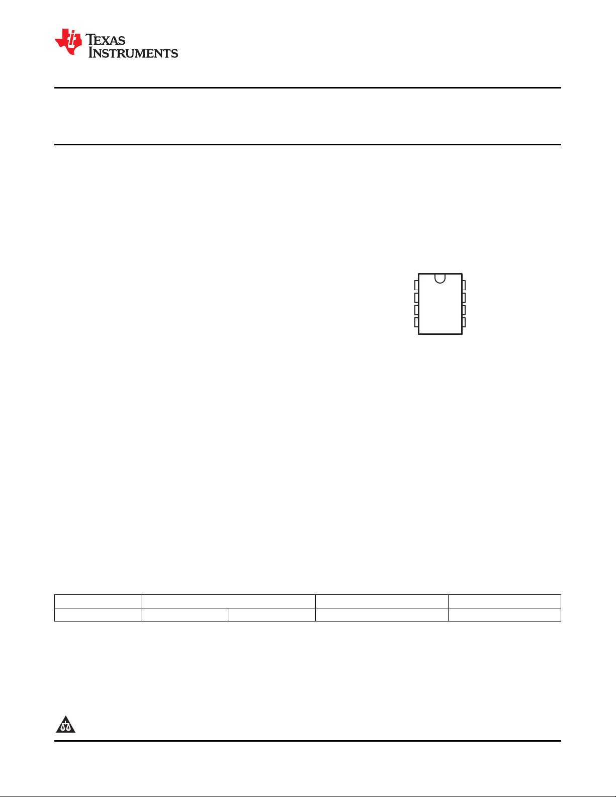
DCU PACKAGE
(TOP VIEW)
1
2
3
4
8
7
6
5
V
CCA
A1
A2
GND
V
CCB
B1
B2
DIR
SN74AVC2T45-Q1
www.ti.com
SCES813 –JUNE 2010
DUAL-BIT DUAL-SUPPLY BUS TRANSCEIVER
WITH CONFIGURABLE VOLTAGE TRANSLATION AND 3-STATE OUTPUTS
Check for Samples: SN74AVC2T45-Q1
1
FEATURES
• Qualified for Automotive Applications
• Control Inputs VIH/VILLevels Are Referenced to
V
Voltage – 8000-V Human-Body Model (A114-A)
CCA
• Fully Configurable Dual-Rail Design Allows – 200-V Machine Model (A115-A)
Each Port to Operate Over the Full 1.2-V to
3.6-V Power-Supply Range
• I/Os Are 4.6-V Tolerant
• I
Supports Partial-Power-Down Mode
off
Operation
• Max Data Rates
– 500 Mbps (1.8-V to 3.3-V Translation)
– 320 Mbps (<1.8-V to 3.3-V Translation)
– 320 Mbps (Translate to 2.5 V or 1.8 V)
– 280 Mbps (Translate to 1.5 V)
– 240 Mbps (Translate to 1.2 V)
• Latch-Up Performance Exceeds 100 mA Per
JESD 78, Class II
• ESD Protection Exceeds JESD 22
– 1000-V Charged-Device Model (C101)
DESCRIPTION
This dual-bit noninverting bus transceiver uses two separate configurable power-supply rails. The A port is
designed to track V
V
CCB
. V
accepts any supply voltage from 1.2 V to 3.6 V. This allows for universal low-voltage bidirectional
CCB
translation between any of the 1.2-V, 1.5-V, 1.8-V, 2.5-V, and 3.3-V voltage nodes.
The SN74AVC2T45 is designed for asynchronous communication between two data buses. The logic levels of
the direction-control (DIR) input activate either the B-port outputs or the A-port outputs. The device transmits data
from the A bus to the B bus when the B-port outputs are activated and from the B bus to the A bus when the
A-port outputs are activated. The input circuitry on both A and B ports always is active and must have a logic
HIGH or LOW level applied to prevent excess ICCand I
The SN74AVC2T45 is designed so that the DIR input is powered by V
This device is fully specified for partial-power-down applications using I
preventing damaging current backflow through the device when it is powered down.
The VCCisolation feature ensures that if either VCCinput is at GND, both ports are in the high-impedance state.
T
A
–40°C to 105°C VSSOP – DCU Reel of 3000 CAVC2T45TDCURQ1 SBUI
(1) For the most current package and ordering information, see the Package Option Addendum at the end of this document, or see the TI
web site at www.ti.com.
(2) Package drawings, thermal data, and symbolization are available at www.ti.com/packaging.
CCA
. V
accepts any supply voltage from 1.2 V to 3.6 V. The B port is designed to track
CCA
.
CCZ
.
CCA
PACKAGE
ORDERING INFORMATION
(2)
ORDERABLE PART NUMBER TOP-SIDE MARKING
(1)
. The I
off
circuitry disables the outputs,
off
1
PRODUCTION DATA information is current as of publication date.
Products conform to specifications per the terms of the Texas
Instruments standard warranty. Production processing does not
necessarily include testing of all parameters.
Please be aware that an important notice concerning availability, standard warranty, and use in critical applications of Texas
Instruments semiconductor products and disclaimers thereto appears at the end of this data sheet.
Copyright © 2010, Texas Instruments Incorporated
B1
DIR
5
7
A1
2
V
CCA
V
CCB
B2
6
A2
3
SN74AVC2T45-Q1
SCES813 –JUNE 2010
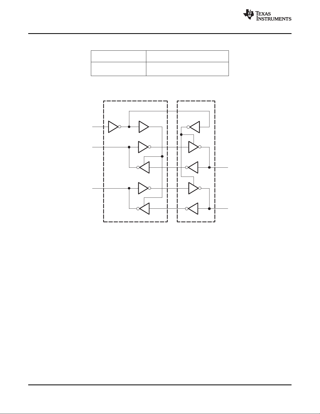
FUNCTION TABLE
(1)
(EACH TRANSCEIVER)
INPUT
DIR
L B data to A bus
H A data to B bus
(1) Input circuits of the data I/Os always are active.
OPERATION
LOGIC DIAGRAM (POSITIVE LOGIC)
www.ti.com
2 Submit Documentation Feedback Copyright © 2010, Texas Instruments Incorporated
Product Folder Link(s): SN74AVC2T45-Q1
SN74AVC2T45-Q1
www.ti.com
ABSOLUTE MAXIMUM RATINGS
(1)
SCES813 –JUNE 2010
over operating free-air temperature range (unless otherwise noted)
MIN MAX UNIT
V
CCA
V
CCB
V
I
V
O
V
O
I
IK
I
OK
I
O
q
JA
T
stg
(1) Stresses beyond those listed under "absolute maximum ratings" may cause permanent damage to the device. These are stress ratings
(2) The input negative-voltage and output voltage ratings may be exceeded if the input and output current ratings are observed.
(3) The output positive-voltage rating may be exceeded up to 4.6 V maximum if the output current ratings are observed.
(4) The package thermal impedance is calculated in accordance with JESD 51-7.
Supply voltage range –0.5 4.6 V
I/O ports (A port) –0.5 4.6
Input voltage range
(2)
I/O ports (B port) –0.5 4.6 V
Control inputs –0.5 4.6
Voltage range applied to any output in the high-impedance or
power-off state
(2)
Voltage range applied to any output in the high or low state
(2) (3)
A port –0.5 4.6
B port –0.5 4.6
A port –0.5 V
B port –0.5 V
CCA
CCB
+ 0.5
+ 0.5
Input clamp current VI< 0 –50 mA
Output clamp current VO< 0 –50 mA
Continuous output current ±50 mA
Continuous current through V
Package thermal impedance
(4)
CCA
, V
, or GND ±100 mA
CCB
DCU package 227 °C/W
Storage temperature range –65 150 °C
only, and functional operation of the device at these or any other conditions beyond those indicated under "recommended operating
conditions" is not implied. Exposure to absolute-maximum-rated conditions for extended periods may affect device reliability.
V
V
Copyright © 2010, Texas Instruments Incorporated Submit Documentation Feedback 3
Product Folder Link(s): SN74AVC2T45-Q1
SN74AVC2T45-Q1
SCES813 –JUNE 2010
RECOMMENDED OPERATING CONDITIONS
V
CCA
V
CCB
V
IH
Supply voltage 1.2 3.6 V
Supply voltage 1.2 3.6 V
High-level
input voltage
Data inputs
(4)
(1)(2)(3)(4)(5)
V
CCI
1.2 V to 1.95 V V
V
CCO
MIN MAX UNIT
× 0.65
CCI
1.95 V to 2.7 V 1.6 V
www.ti.com
2.7 V to 3.6 V 2
V
IL
Low-level
input voltage
Data inputs
(4)
1.95 V to 2.7 V 0.7 V
1.2 V to 1.95 V V
CCI
× 0.35
2.7 V to 3.6 V 0.8
V
IH
High-level DIR
input voltage (referenced to V
CCA
(5)
)
1.95 V to 2.7 V 1.6 V
2.7 V to 3.6 V 2
1.2 V to 1.95 V V
1.2 V to 1.95 V V
V
IL
V
I
V
O
Low-level DIR
input voltage (referenced to V
CCA
(5)
)
1.95 V to 2.7 V 0.7 V
2.7 V to 3.6 V 0.8
Input voltage 0 3.6 V
Output voltage V
Active state 0 V
3-state 0 3.6
CCA
× 0.65
CCA
× 0.35
CCO
1.2 V –3
1.4 V to 1.6 V –6
I
OH
High-level output current 1.65 V to 1.95 V –8 mA
2.3 V to 2.7 V –9
3 V to 3.6 V –12
1.2 V 3
1.4 V to 1.6 V 6
I
OL
Low-level output current 1.65 V to 1.95 V 8 mA
2.3 V to 2.7 V 9
3 V to 3.6 V 12
Δt/Δv Input transition rise or fall rate 5 ns/V
T
A
(1) V
(2) V
(3) All unused data inputs of the device must be held at V
(4) For V
(5) For V
Operating free-air temperature –40 105 °C
is the VCCassociated with the input port.
CCI
is the VCCassociated with the output port.
CCO
Implications of Slow or Floating CMOS Inputs, literature number SCBA004.
values not specified in the data sheet, VIHmin = V
CCI
values not specified in the data sheet, VIHmin = V
CCI
or GND to ensure proper device operation. See the TI application report,
CCI
× 0.7 V, VILmax = V
CCI
× 0.7 V, VILmax = V
CCA
CCI
CCA
× 0.3 V.
× 0.3 V.
4 Submit Documentation Feedback Copyright © 2010, Texas Instruments Incorporated
Product Folder Link(s): SN74AVC2T45-Q1

SN74AVC2T45-Q1
www.ti.com
ELECTRICAL CHARACTERISTICS
(1)(2)
over recommended operating free-air temperature range (unless otherwise noted)
PARAMETER TEST CONDITIONS V
CCA
V
CCB
IOH= –100 mA 1.2 V to 3.6 V 1.2 V to 3.6 V V
IOH= –3 mA 1.2 V 1.2 V 0.95
V
OH
IOH= –6 mA 1.4 V 1.4 V 1.05
IOH= –8 mA 1.65 V 1.65 V 1.2
VI= V
IH
IOH= –9 mA 2.3 V 2.3 V 1.75
IOH= –12 mA 3 V 3 V 2.3
IOL= 100 mA 1.2 V to 3.6 V 1.2 V to 3.6 V 0.2
IOL= 3 mA 1.2 V 1.2 V 0.25
V
OL
IOL= 6 mA 1.4 V 1.4 V 0.35
IOL= 8 mA 1.65 V 1.65 V 0.45
VI= V
IL
IOL= 9 mA 2.3 V 2.3 V 0.55
IOL= 12 mA 3 V 3 V 0.7
I
DIR VI= V
I
A port 0 V 0 to 3.6 V ±0.1 ±1 ±5
I
off
B port 0 to 3.6 V 0 V ±0.1 ±1 ±5
B port 0 V 3.6 V ±0.5 ±2.5 ±5
I
OZ
A port 3.6 V 0 V ±0.5 ±2.5 ±5
VIor VO= 0 to 3.6 V mA
VO= V
VI= V
or GND 1.2 V to 3.6 V 1.2 V to 3.6 V ±0.025 ±0.25 ±1 mA
CCA
or GND,
CCO
or GND
CCI
1.2 V to 3.6 V 1.2 V to 3.6 V 10
I
CCA
VI= V
or GND, IO= 0 0 V 3.6 V –2 mA
CCI
3.6 V 0 V 10
1.2 V to 3.6 V 1.2 V to 3.6 V 10
I
CCB
VI= V
or GND, IO= 0 0 V 3.6 V 10 mA
CCI
3.6 V 0 V –2
I
+ I
CCA
CCB
(see Table 1)
Control
C
I
inputs
A or B
C
io
port
(1) V
CCO
(2) V
CCI
VI= V
or GND, IO= 0 1.2 V to 3.6 V 1.2 V to 3.6 V 20 mA
CCI
VI= 3.3 V or GND 3.3 V 3.3 V 2.5 pF
VO= 3.3 V or GND 3.3 V 3.3 V 6 pF
is the VCCassociated with the output port.
is the VCCassociated with the input port.
TA= 25°C –40°C to 105°C
MIN TYP MAX MIN MAX
CCO
SCES813 –JUNE 2010
UNIT
– 0.2 V
V
V
mA
Copyright © 2010, Texas Instruments Incorporated Submit Documentation Feedback 5
Product Folder Link(s): SN74AVC2T45-Q1
SN74AVC2T45-Q1
SCES813 –JUNE 2010
www.ti.com
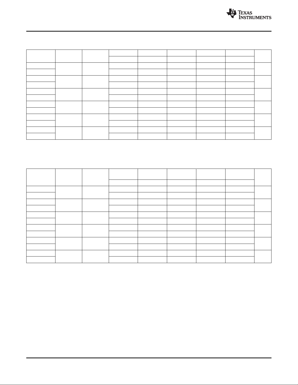
SWITCHING CHARACTERISTICS
over recommended operating free-air temperature range, V
V
= 1.2 V V
PARAMETER UNIT
t
PLH
t
PHL
t
PLH
t
PHL
t
PHZ
t
PLZ
t
PHZ
t
PLZ
(1)
t
PZH
(1)
t
PZL
(1)
t
PZH
(1)
t
PZL
FROM TO
(INPUT) (OUTPUT)
A B ns
B A ns
DIR A ns
DIR B ns
DIR A ns
DIR B ns
(1) The enable time is a calculated value, derived using the formula shown in the enable times section.
CCB
TYP TYP TYP TYP TYP
3.1 2.6 2.4 2.2 2.2
3.1 2.6 2.4 2.2 2.2
3.4 3.1 3 2.9 2.9
3.4 3.1 3 2.9 2.9
5.2 5.2 5.1 5 4.8
5.2 5.2 5.1 5 4.8
5 4 3.8 2.8 3.2
5 4 3.8 2.8 3.2
8.4 7.1 6.8 5.7 6.1
8.4 7.1 6.8 5.7 6.1
8.3 7.8 7.5 7.2 7
8.3 7.8 7.5 7.2 7
= 1.2 V (see Figure 1)
CCA
= 1.5 V V
CCB
= 1.8 V V
CCB
= 2.5 V V
CCB
CCB
= 3.3 V
SWITCHING CHARACTERISTICS
over recommended operating free-air temperature range, V
V
= 1.2 V
PARAMETER UNIT
t
PLH
t
PHL
t
PLH
t
PHL
t
PHZ
t
PLZ
t
PHZ
t
PLZ
(1)
t
PZH
(1)
t
PZL
(1)
t
PZH
(1)
t
PZL
FROM TO
(INPUT) (OUTPUT)
A B ns
B A ns
DIR A ns
DIR B ns
DIR A ns
DIR B ns
(1) The enable time is a calculated value, derived using the formula shown in the enable times section.
CCB
TYP MIN MAX MIN MAX MIN MAX MIN MAX
2.8 0.7 5.6 0.5 4.8 0.4 3.9 0.3 3.7
2.8 0.7 5.6 0.5 4.8 0.4 3.9 0.3 3.7
2.7 0.8 5.6 0.7 5.4 0.6 5.1 0.5 4.9
2.7 0.8 5.6 0.7 5.4 0.6 5.1 0.5 4.9
3.9 1.3 8.7 1.3 8 1.1 7.9 1.4 7.8
3.9 1.3 8.7 1.3 8 1.1 7.9 1.4 7.8
4.7 1.1 7.2 1.4 7.1 1.2 7.1 1.7 7.3
4.7 1.1 7.2 1.4 7.1 1.2 7.1 1.7 7.3
7.4 12.6 12.3 12 12
7.4 12.6 12.3 12 12
6.7 14.1 12.6 11.6 11.3
6.7 14.1 12.6 11.6 11.3
= 1.5 V ± 0.1 V (see Figure 1)
CCA
V
= 1.5 V V
CCB
± 0.1 V ± 0.15 V ± 0.2 V ± 0.3 V
= 1.8 V V
CCB
= 2.5 V V
CCB
CCB
= 3.3 V
6 Submit Documentation Feedback Copyright © 2010, Texas Instruments Incorporated
Product Folder Link(s): SN74AVC2T45-Q1
SN74AVC2T45-Q1
www.ti.com
SCES813 –JUNE 2010
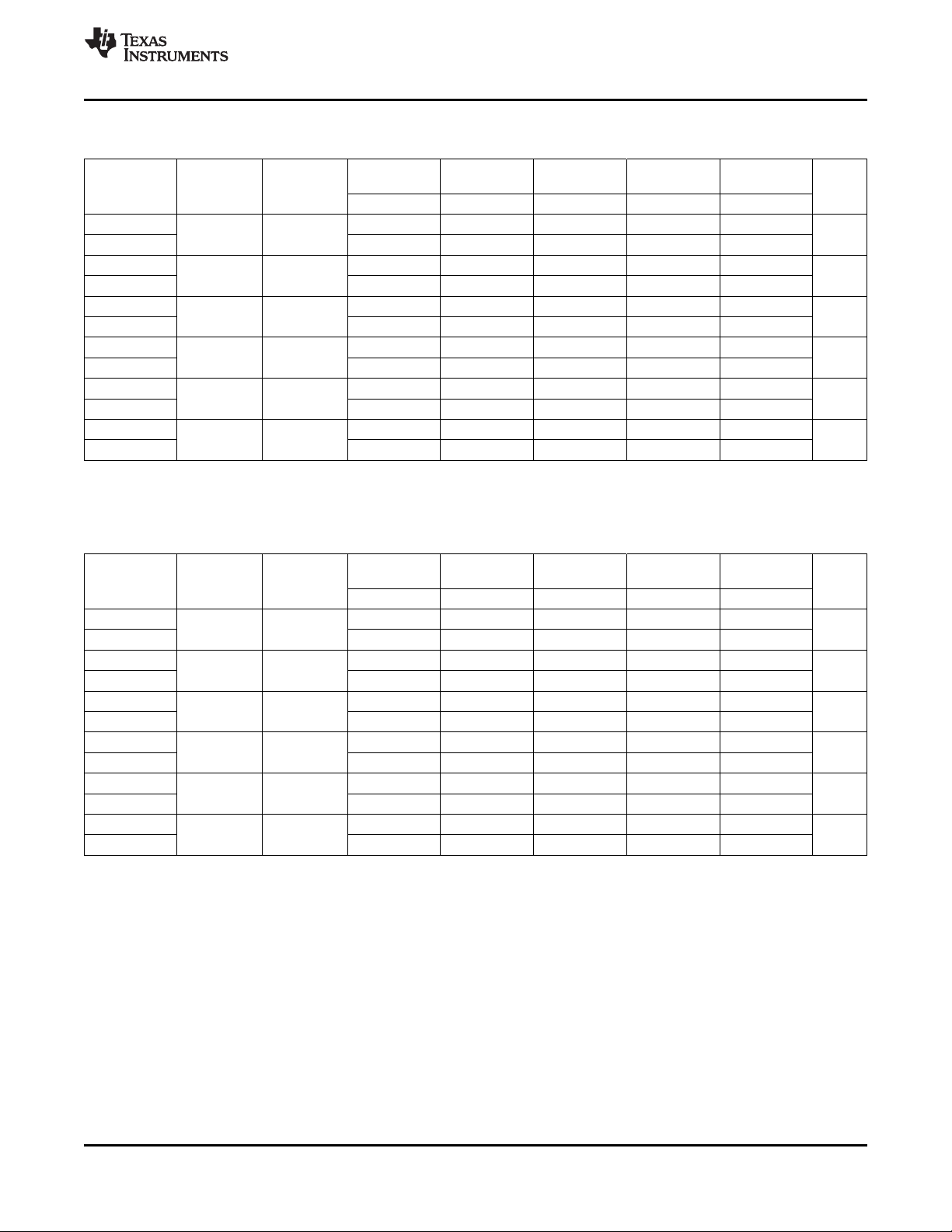
SWITCHING CHARACTERISTICS
over recommended operating free-air temperature range, V
V
= 1.2 V
PARAMETER UNIT
t
PLH
t
PHL
t
PLH
t
PHL
t
PHZ
t
PLZ
t
PHZ
t
PLZ
(1)
t
PZH
(1)
t
PZL
(1)
t
PZH
(1)
t
PZL
FROM TO
(INPUT) (OUTPUT)
A B ns
B A ns
DIR A ns
DIR B ns
DIR A ns
DIR B ns
(1) The enable time is a calculated value, derived using the formula shown in the enable times section.
CCB
TYP MIN MAX MIN MAX MIN MAX MIN MAX
2.7 0.5 5.4 0.4 4.5 0.2 3.6 0.2 3.3
2.7 0.5 5.4 0.4 4.5 0.2 3.6 0.2 3.3
2.4 0.7 4.9 0.5 4.6 0.5 4.2 0.4 4
2.4 0.7 4.9 0.5 4.6 0.5 4.2 0.4 4
3.7 1.3 8.3 0.7 7.1 1.4 5.5 1.1 5.4
3.7 1.3 8.3 0.7 7.1 1.4 5.5 1.1 5.4
4.4 1.3 6 1.3 6.1 0.8 5.9 1.5 6.1
4.4 1.3 6 1.3 6.1 0.8 5.9 1.5 6.1
6.8 10.7 10.5 9.9 9.9
6.8 10.7 10.5 9.9 9.9
6.4 13.5 11.4 8.9 8.5
6.4 13.5 11.4 8.9 8.5
= 1.8 V ± 0.15 V (see Figure 1)
CCA
V
= 1.5 V V
CCB
± 0.1 V ± 0.15 V ± 0.2 V ± 0.3 V
= 1.8 V V
CCB
= 2.5 V V
CCB
CCB
= 3.3 V
SWITCHING CHARACTERISTICS
over recommended operating free-air temperature range, V
V
= 1.2 V
PARAMETER UNIT
t
PLH
t
PHL
t
PLH
t
PHL
t
PHZ
t
PLZ
t
PHZ
t
PLZ
(1)
t
PZH
(1)
t
PZL
(1)
t
PZH
(1)
t
PZL
FROM TO
(INPUT) (OUTPUT)
A B ns
B A ns
DIR A ns
DIR B ns
DIR A ns
DIR B ns
(1) The enable time is a calculated value, derived using the formula shown in the enable times section.
CCB
TYP MIN MAX MIN MAX MIN MAX MIN MAX
2.6 0.4 5.1 0.2 4.2 0.2 3.2 0.2 2.8
2.6 0.4 5.1 0.2 4.2 0.2 3.2 0.2 2.8
2.1 0.6 4 0.5 3.6 0.4 3.2 0.3 3
2.1 0.6 4 0.5 3.6 0.4 3.2 0.3 3
2.4 0.7 8.1 0.8 6.6 0.8 5.2 0.5 4.5
2.4 0.7 8.1 0.8 6.6 0.8 5.2 0.5 4.5
3.8 1 4.5 0.6 4.5 0.5 4.4 1.1 4.3
3.8 1 4.5 0.6 4.5 0.5 4.4 1.1 4.3
5.9 8.7 7.9 7.4 7.1
5.9 8.7 7.9 7.4 7.1
5 13 10.6 8.2 7.1
5 13 10.6 8.2 7.1
= 2.5 V ± 0.2 V (see Figure 1)
CCA
V
= 1.5 V V
CCB
± 0.1 V ± 0.15 V ± 0.2 V ± 0.3 V
= 1.8 V V
CCB
= 2.5 V V
CCB
CCB
= 3.3 V
Copyright © 2010, Texas Instruments Incorporated Submit Documentation Feedback 7
Product Folder Link(s): SN74AVC2T45-Q1
 Loading...