

Texas Instruments SN74AVC16834DGGR, SN74AVC16834DGVR Datasheet
SN74AVC16834
18-BIT UNIVERSAL BUS DRIVER
WITH 3-STATE OUTPUTS
SCES183F – DECEMBER 1998 – REVISED FEBRUARY 2000
1
POST OFFICE BOX 655303 • DALLAS, TEXAS 75265
D
Member of the Texas Instruments
Widebus
Family
D
EPIC
(Enhanced-Performance Implanted
CMOS) Submicron Process
D
DOC
(Dynamic Output Control) Circuit
Dynamically Changes Output Impedance,
Resulting in Noise Reduction Without
Speed Degradation
D
Dynamic Drive Capability Is Equivalent to
Standard Outputs With IOH and IOL of
±24 mA at 2.5-V V
CC
D
Overvoltage-Tolerant Inputs/Outputs Allow
Mixed-Voltage-Mode Data Communications
D
I
off
Supports Partial-Power-Down Mode
Operation
D
Ideal for Use in PC133 Registered DIMM
Applications
D
ESD Protection Exceeds JESD 22
– 2000-V Human-Body Model (A114-A)
– 200-V Machine Model (A115-A)
D
Latch-Up Performance Exceeds 100 mA Per
JESD 78, Class II
D
Package Options Include Plastic Thin
Shrink Small-Outline (DGG) and Thin Very
Small-Outline (DGV) Packages
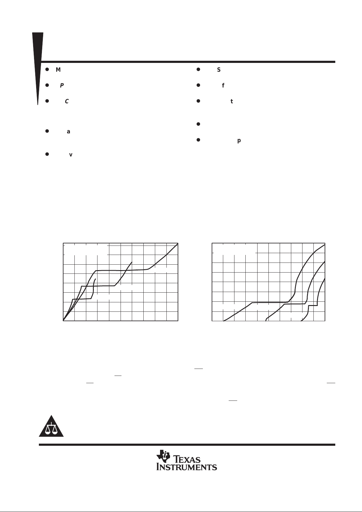
description
A Dynamic Output Control (DOC) circuit is implemented, which, during the transition, initially lowers the output
impedance to effectively drive the load and, subsequently, raises the impedance to reduce noise. Figure 1
shows typical V
OL
vs IOL and VOH vs IOH curves to illustrate the output impedance and drive capability of the
circuit. At the beginning of the signal transition, the DOC circuit provides a maximum dynamic drive that is
equivalent to a high-drive standard-output device. For more information, refer to the TI application reports,
AVC
Logic Family T echnology and Applications
, literature number SCEA006, and
Dynamic Output Control (DOC)
Circuitry Technology and Applications
, literature number SCEA009.
136
–128–144–160
0.4
0.8
1.2
1.6
2.0
2.4
2.8
17015311910285685134170
0.4
0.8
1.2
1.6
2.0
2.4
2.8
3.2
TA = 25°C
Process = Nominal
IOL – Output Current – mA
VCC = 3.3 V
VCC = 2.5 V
VCC = 1.8 V
– Output Voltage – V
OL
V
TA = 25°C
Process = Nominal
IOH – Output Current – mA
VCC = 3.3 V
VCC = 2.5 V
VCC = 1.8 V
– Output Voltage – V
OH
V
–80–96–112 –32–48–64 0–16
Figure 1. Output Voltage vs Output Current
This 18-bit universal bus driver is operational at 1.2-V to 3.6-V VCC, but is designed specifically for 1.65-V to
3.6-V VCC operation.
Data flow from A to Y is controlled by the output-enable (OE
) input. The device operates in the transparent mode
when the latch-enable (LE
) input is low. The A data is latched if the clock (CLK) input is held at a high or low
logic level. If LE is high, the A data is stored in the latch/flip-flop on the low-to-high transition of CLK. When OE
is high, the outputs are in the high-impedance state.
T o ensure the high-impedance state during power up or power down, OE should be tied to VCC through a pullup
resistor; the minimum value of the resistor is determined by the current-sinking capability of the driver.
Copyright 2000, Texas Instruments Incorporated
Please be aware that an important notice concerning availability, standard warranty, and use in critical applications of
Texas Instruments semiconductor products and disclaimers thereto appears at the end of this data sheet.
DOC, EPIC, and Widebus are trademarks of Texas Instruments Incorporated.
PRODUCTION DATA information is current as of publication date.
Products conform to specifications per the terms of Texas Instruments
standard warranty. Production processing does not necessarily include
testing of all parameters.
SN74AVC16834
18-BIT UNIVERSAL BUS DRIVER
WITH 3-STATE OUTPUTS
SCES183F – DECEMBER 1998 – REVISED FEBRUARY 2000
2
POST OFFICE BOX 655303 • DALLAS, TEXAS 75265
description (continued)
This device is fully specified for partial-power-down applications using I
off
. The I
off
circuitry disables the outputs,
preventing damaging current backflow through the device when it is powered down.
The SN74AVC16834 is characterized for operation from –40°C to 85°C.
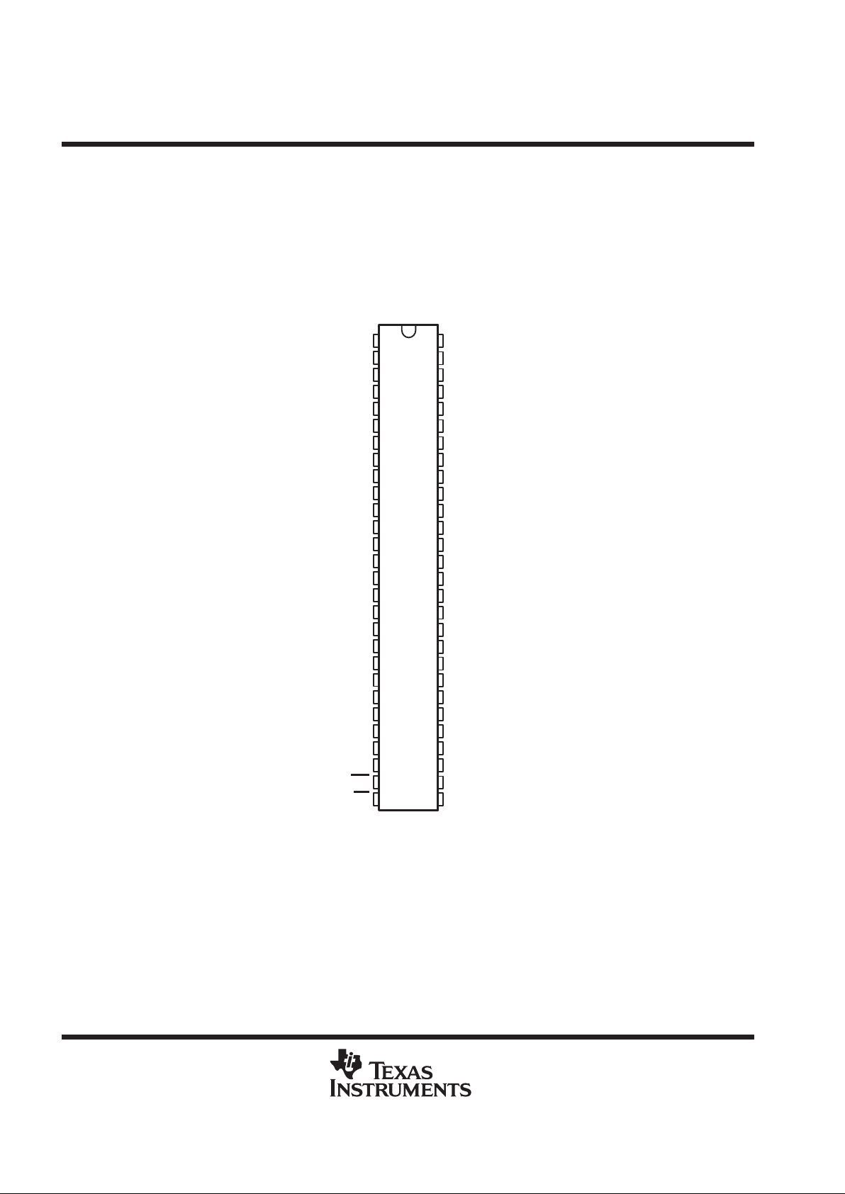
terminal assignments
DGG OR DGV PACKAGE
(TOP VIEW)
1
2
3
4
5
6
7
8
9
10
11
12
13
14
15
16
17
18
19
20
21
22
23
24
25
26
27
28
56
55
54
53
52
51
50
49
48
47
46
45
44
43
42
41
40
39
38
37
36
35
34
33
32
31
30
29
NC
NC
Y1
GND
Y2
Y3
V
CC
Y4
Y5
Y6
GND
Y7
Y8
Y9
Y10
Y11
Y12
GND
Y13
Y14
Y15
V
CC
Y16
Y17
GND
Y18
OE
LE
GND
NC
A1
GND
A2
A3
V
CC
A4
A5
A6
GND
A7
A8
A9
A10
A11
A12
GND
A13
A14
A15
V
CC
A16
A17
GND
A18
CLK
GND
NC – No internal connection
SN74AVC16834
18-BIT UNIVERSAL BUS DRIVER
WITH 3-STATE OUTPUTS
SCES183F – DECEMBER 1998 – REVISED FEBRUARY 2000
3
POST OFFICE BOX 655303 • DALLAS, TEXAS 75265
FUNCTION TABLE
(each universal bus driver)
INPUTS
OUTPUT
OE LE CLK A
Y
H X X X Z
L LXL L
L LXH H
L H ↑ LL
L H ↑ HH
L HHX Y
0
†
L H L X Y
0
‡
†
Output level before the indicated steady-state
input conditions were established, provided
that CLK is high before LE
goes high
‡
Output level before the indicated steady-state
input conditions were established
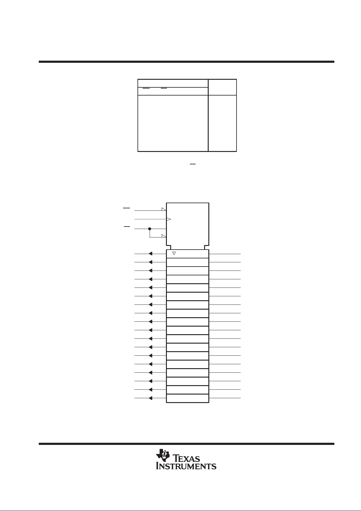
logic symbol
§
A6
47
A7
45
A8
44
A9
43
A10
42
A11
41
A12
40
A13
38
A14
37
A15
36
A16
34
A17
33
A18
31
OE
EN1
27
30
CLK
3
Y1
5
Y2
6
Y3
9
Y5
10
Y6
12
Y7
13
Y8
14
Y9
15
Y10
16
Y11
17
Y12
19
Y13
20
Y14
21
Y15
23
Y16
24
Y17
26
Y18
C3
28
G2
§
This symbol is in accordance with ANSI/IEEE Std 91-1984 and IEC Publication 617-12.
A1
54
A2
52
A3
51
A4
49
A5
48
2C3
8
Y4
LE
1
3D1
SN74AVC16834
18-BIT UNIVERSAL BUS DRIVER
WITH 3-STATE OUTPUTS
SCES183F – DECEMBER 1998 – REVISED FEBRUARY 2000
4
POST OFFICE BOX 655303 • DALLAS, TEXAS 75265
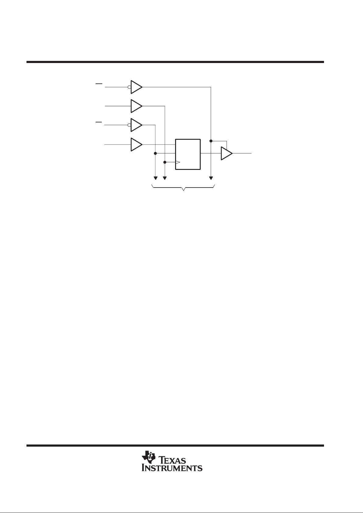
logic diagram (positive logic)
OE
CLK
Y1
1D
C1
CLK
To 17 Other Channels
LE
A1
27
30
28
54
3
absolute maximum ratings over operating free-air temperature range (unless otherwise noted)
†
Supply voltage range, VCC –0.5 V to 4.6 V. . . . . . . . . . . . . . . . . . . . . . . . . . . . . . . . . . . . . . . . . . . . . . . . . . . . . . . . .
Input voltage range, VI (see Note 1) –0.5 V to 4.6 V. . . . . . . . . . . . . . . . . . . . . . . . . . . . . . . . . . . . . . . . . . . . . . . . .
Voltage range applied to any output in the high-impedance or power-off state, V
O
(see Note 1) –0.5 V to 4.6 V. . . . . . . . . . . . . . . . . . . . . . . . . . . . . . . . . . . . . . . . . . . . . . . . . . . . . . . . . . . . . . . . . . .
Voltage range applied to any output in the high or low state, V
O
(see Notes 1 and 2) –0.5 V to VCC + 0.5 V. . . . . . . . . . . . . . . . . . . . . . . . . . . . . . . . . . . . . . . . . . . . . . . . . . . . . . .
Input clamp current, IIK (VI < 0) –50 mA. . . . . . . . . . . . . . . . . . . . . . . . . . . . . . . . . . . . . . . . . . . . . . . . . . . . . . . . . . .
Output clamp current, IOK (VO < 0) –50 mA. . . . . . . . . . . . . . . . . . . . . . . . . . . . . . . . . . . . . . . . . . . . . . . . . . . . . . . .
Continuous output current, I
O
±50 mA. . . . . . . . . . . . . . . . . . . . . . . . . . . . . . . . . . . . . . . . . . . . . . . . . . . . . . . . . . . . .
Continuous current through each VCC or GND ±100 mA. . . . . . . . . . . . . . . . . . . . . . . . . . . . . . . . . . . . . . . . . . . . .
Package thermal impedance, θJA (see Note 3): DGG package 64°C/W. . . . . . . . . . . . . . . . . . . . . . . . . . . . . . .
DGV package 48°C/W. . . . . . . . . . . . . . . . . . . . . . . . . . . . . . . .
Storage temperature range, T
stg
–65°C to 150°C. . . . . . . . . . . . . . . . . . . . . . . . . . . . . . . . . . . . . . . . . . . . . . . . . . .
†
Stresses beyond those listed under “absolute maximum ratings” may cause permanent damage to the device. These are stress ratings only, and
functional operation of the device at these or any other conditions beyond those indicated under “recommended operating conditions” is not
implied. Exposure to absolute-maximum-rated conditions for extended periods may affect device reliability.
NOTES: 1. The input and output negative-voltage ratings may be exceeded if the input and output current ratings are observed.
2. The output positive-voltage rating may be exceeded up to 4.6 V maximum if the output current rating is observed.
3. The package thermal impedance is calculated in accordance with JESD 51.
 Loading...