

Please be aware that an important notice concerning availability, standard warranty, and use in critical applications of
Texas Instruments semiconductor products and disclaimers thereto appears at the end of this data sheet.
SN74A VC16373
16-BIT TRANSPARENT D-TYPE LATCH
WITH 3-STATE OUTPUTS
SCES156F – DECEMBER 1998 – REVISED FEBRUARY 2000
1
POST OFFICE BOX 655303 • DALLAS, TEXAS 75265
D
Member of the Texas Instruments
Widebus
Family
D
EPIC
(Enhanced-Performance Implanted
CMOS) Submicron Process
D
DOC
(Dynamic Output Control) Circuit
Dynamically Changes Output Impedance,
Resulting in Noise Reduction Without
Speed Degradation
D
Dynamic Drive Capability Is Equivalent to
Standard Outputs With IOH and IOL of
±24 mA at 2.5-V V
CC
D
Overvoltage-Tolerant Inputs/Outputs Allow
Mixed-Voltage-Mode Data Communications
D
I
off
Supports Partial-Power-Down Mode
Operation
D
ESD Protection Exceeds JESD 22
– 2000-V Human-Body Model (A114-A)
– 200-V Machine Model (A115-A)
D
Latch-Up Performance Exceeds 100 mA Per
JESD 78, Class II
D
Package Options Include Plastic Thin
Shrink Small-Outline (DGG) and Thin Very
Small-Outline (DGV) Packages
description
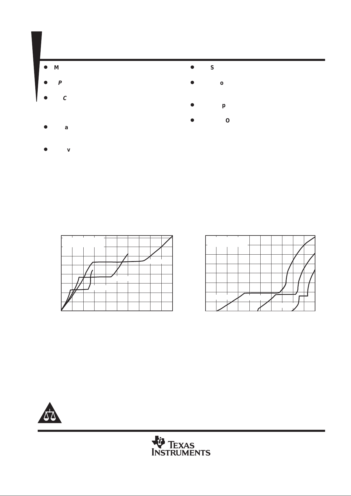
A Dynamic Output Control (DOC) circuit is implemented, which, during the transition, initially lowers the output
impedance to effectively drive the load and, subsequently, raises the impedance to reduce noise. Figure 1
shows typical V
OL
vs IOL and VOH vs IOH curves to illustrate the output impedance and drive capability of the
circuit. At the beginning of the signal transition, the DOC circuit provides a maximum dynamic drive that is
equivalent to a high-drive standard-output device. For more information, refer to the TI application reports,
AVC
Logic Family T echnology and Applications
, literature number SCEA006, and
Dynamic Output Control (DOC)
Circuitry Technology and Applications
, literature number SCEA009.
136
–128–144–160
0.4
0.8
1.2
1.6
2.0
2.4
2.8
17015311910285685134170
0.4
0.8
1.2
1.6
2.0
2.4
2.8
3.2
TA = 25°C
Process = Nominal
IOL – Output Current – mA
VCC = 3.3 V
VCC = 2.5 V
VCC = 1.8 V
– Output Voltage – V
OL
V
TA = 25°C
Process = Nominal
IOH – Output Current – mA
VCC = 3.3 V
VCC = 2.5 V
VCC = 1.8 V
– Output Voltage – V
OH
V
–80–96–112 –32–48–64 0–16
Figure 1. Output Voltage vs Output Current
This 16-bit transparent D-type latch is operational at 1.2-V to 3.6-V VCC, but is designed specifically for 1.65-V
to 3.6-V VCC operation.
The SN74AVC16373 is particularly suitable for implementing buffer registers, I/O ports, bidirectional bus
drivers, and working registers. This device can be used as two 8-bit latches or one 16-bit latch. When the
latch-enable (LE) input is high, the Q outputs follow the data (D) inputs. When LE is taken low, the Q outputs
are latched at the levels set up at the D inputs.
PRODUCTION DATA information is current as of publication date.
Products conform to specifications per the terms of Texas Instruments
standard warranty. Production processing does not necessarily include
testing of all parameters.
Copyright 2000, Texas Instruments Incorporated
DOC, EPIC, and Widebus are trademarks of Texas Instruments Incorporated.
SN74AVC16373
16-BIT TRANSPARENT D-TYPE LATCH
WITH 3-STATE OUTPUTS
SCES156F – DECEMBER 1998 – REVISED FEBRUARY 2000
2
POST OFFICE BOX 655303 • DALLAS, TEXAS 75265
description (continued)
A buffered output-enable (OE) input can be used to place the eight outputs in either a normal logic state (high
or low logic levels) or the high-impedance state. In the high-impedance state, the outputs neither load nor drive
the bus lines significantly . The high-impedance state and the increased drive provide the capability to drive bus
lines without need for interface or pullup components. OE
does not affect internal operations of the latch. Old
data can be retained or new data can be entered while the outputs are in the high-impedance state.
T o ensure the high-impedance state during power up or power down, OE should be tied to VCC through a pullup
resistor; the minimum value of the resistor is determined by the current-sinking capability of the driver.
This device is fully specified for partial-power-down applications using I
off
. The I
off
circuitry disables the outputs,
preventing damaging current backflow through the device when it is powered down.
The SN74AVC16373 is characterized for operation from –40°C to 85°C.
terminal assignments
DGG OR DGV PACKAGE
(TOP VIEW)
1
2
3
4
5
6
7
8
9
10
11
12
13
14
15
16
17
18
19
20
21
22
23
24
48
47
46
45
44
43
42
41
40
39
38
37
36
35
34
33
32
31
30
29
28
27
26
25
1OE
1Q1
1Q2
GND
1Q3
1Q4
V
CC
1Q5
1Q6
GND
1Q7
1Q8
2Q1
2Q2
GND
2Q3
2Q4
V
CC
2Q5
2Q6
GND
2Q7
2Q8
2OE
1LE
1D1
1D2
GND
1D3
1D4
V
CC
1D5
1D6
GND
1D7
1D8
2D1
2D2
GND
2D3
2D4
V
CC
2D5
2D6
GND
2D7
2D8
2LE
SN74AVC16373
16-BIT TRANSPARENT D-TYPE LATCH
WITH 3-STATE OUTPUTS
SCES156F – DECEMBER 1998 – REVISED FEBRUARY 2000
3
POST OFFICE BOX 655303 • DALLAS, TEXAS 75265
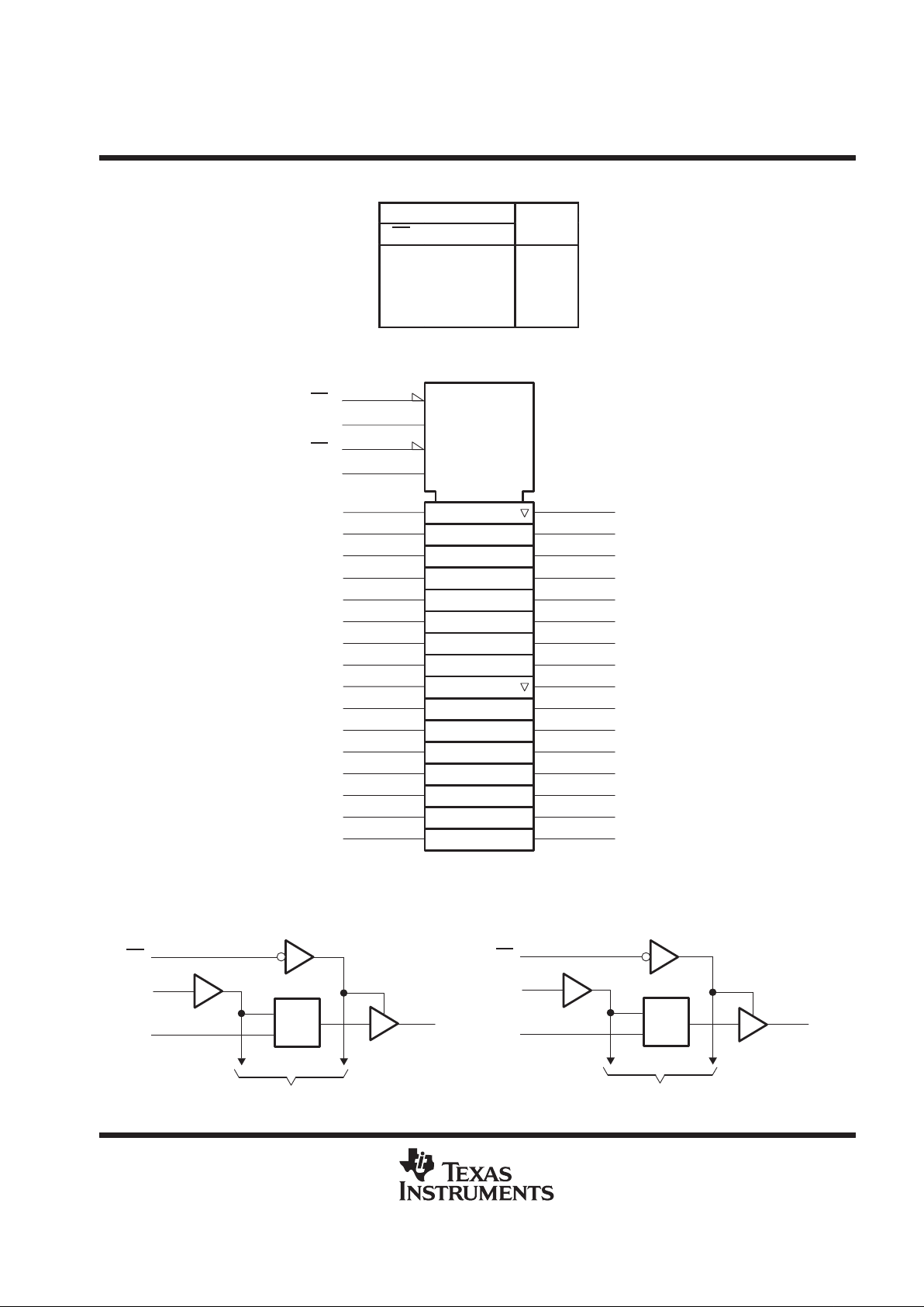
FUNCTION TABLE
(each 8-bit latch)
INPUTS
OUTPUT
OE
LE D
Q
L H H H
L HL L
L LX Q
0
H X X Z
logic symbol
†
†
This symbol is in accordance with ANSI/IEEE Std 91-1984 and IEC Publication 617-12.
1OE
2OE
1EN
1
C3
48
1LE
3D
47
1D1
46
1D2
44
1D3
43
1D4
1Q1
2
1Q2
3
1Q3
5
1Q4
6
41
1D5
40
1D6
38
1D7
37
1D8
1Q5
8
1Q6
9
1Q7
11
1Q8
12
4D
36
2D1
35
2D2
33
2D3
32
2D4
2Q1
13
2Q2
14
2Q3
16
2Q4
17
30
2D5
29
2D6
27
2D7
26
2D8
2Q5
19
2Q6
20
2Q7
22
2Q8
23
2EN
24
C4
25
2LE
1
2
logic diagram (positive logic)
1OE
1LE
1D1
To Seven Other Channels
1Q1
2OE
2LE
2D1
2Q1
To Seven Other Channels
1
48
47
24
25
36
C1
1D
132
C1
1D

SN74AVC16373
16-BIT TRANSPARENT D-TYPE LATCH
WITH 3-STATE OUTPUTS
SCES156F – DECEMBER 1998 – REVISED FEBRUARY 2000
4
POST OFFICE BOX 655303 • DALLAS, TEXAS 75265
absolute maximum ratings over operating free-air temperature range (unless otherwise noted)
†
Supply voltage range, VCC –0.5 V to 4.6 V. . . . . . . . . . . . . . . . . . . . . . . . . . . . . . . . . . . . . . . . . . . . . . . . . . . . . . . . .
Input voltage range, VI (see Note 1) –0.5 V to 4.6 V. . . . . . . . . . . . . . . . . . . . . . . . . . . . . . . . . . . . . . . . . . . . . . . . .
Voltage range applied to any output in the high-impedance or power-off state, V
O
(see Note 1) –0.5 V to 4.6 V. . . . . . . . . . . . . . . . . . . . . . . . . . . . . . . . . . . . . . . . . . . . . . . . . . . . . . . . . . . . . . . . . . .
Voltage range applied to any output in the high or low state, V
O
(see Notes 1 and 2) –0.5 V to VCC + 0.5 V. . . . . . . . . . . . . . . . . . . . . . . . . . . . . . . . . . . . . . . . . . . . . . . . . . . . . . .
Input clamp current, IIK (VI < 0) –50 mA. . . . . . . . . . . . . . . . . . . . . . . . . . . . . . . . . . . . . . . . . . . . . . . . . . . . . . . . . . .
Output clamp current, I
OK
(VO < 0) –50 mA. . . . . . . . . . . . . . . . . . . . . . . . . . . . . . . . . . . . . . . . . . . . . . . . . . . . . . . .
Continuous output current, IO ±50 mA. . . . . . . . . . . . . . . . . . . . . . . . . . . . . . . . . . . . . . . . . . . . . . . . . . . . . . . . . . . . .
Continuous current through each VCC or GND ±100 mA. . . . . . . . . . . . . . . . . . . . . . . . . . . . . . . . . . . . . . . . . . . . .
Package thermal impedance, θJA (see Note 3): DGG package 70°C/W. . . . . . . . . . . . . . . . . . . . . . . . . . . . . . .
DGV package 58°C/W. . . . . . . . . . . . . . . . . . . . . . . . . . . . . . . .
Storage temperature range, T
stg
–65°C to 150°C. . . . . . . . . . . . . . . . . . . . . . . . . . . . . . . . . . . . . . . . . . . . . . . . . . .
†
Stresses beyond those listed under “absolute maximum ratings” may cause permanent damage to the device. These are stress ratings only, and
functional operation of the device at these or any other conditions beyond those indicated under “recommended operating conditions” is not
implied. Exposure to absolute-maximum-rated conditions for extended periods may affect device reliability.
NOTES: 1. The input and output negative-voltage ratings may be exceeded if the input and output current ratings are observed.
2. The output positive-voltage rating may be exceeded up to 4.6 V maximum if the output current rating is observed.
3. The package thermal impedance is calculated in accordance with JESD 51.
 Loading...