

SN74AS4374B
OCTAL EDGE-TRIGGERED D-TYPE DUAL-RANK FLIP-FLOP
WITH 3-STATE OUTPUTS
SDAS109D – APRIL 1989 – REVISED JANUARY 1995
Copyright 1995, Texas Instruments Incorporated
1
POST OFFICE BOX 655303 • DALLAS, TEXAS 75265
• 3-State Outputs Drive Bus Lines Directly
• Package Options Include Plastic
Small-Outline (DW) Packages and Standard
Plastic (N) 300-mil DIPs
description
This 8-bit flip-flop features 3-state outputs
designed specifically for driving highly capacitive
or relatively low-impedance loads. It is particularly
suitable for implementing buffer registers, I/O
ports, bidirectional bus drivers, and working
registers.
The eight flip-flops of the SN74AS4374B are
edge-triggered D-type flip-flops. On the second
positive transition of the clock (CLK) input, the Q
outputs are set to the logic levels set up at the data
(D) inputs.
The output-enable (OE
) input does not affect internal operations of the flip-flops. Previously stored data can be
retained or new data can be entered while the outputs are in the high-impedance state.
The SN74AS4374B is characterized for operation from 0°C to 70°C.
FUNCTION TABLE
(each flip-flop)
INPUTS
OUTPUT
OE CLK D
†
Q
H X X Z
L ↑ LL
L↑HH
LLXQ
0
†
Data presented at the D inputs require
two clock cycles to appear at the Q
outputs.
1
2
3
4
5
6
7
8
9
10
20
19
18
17
16
15
14
13
12
11
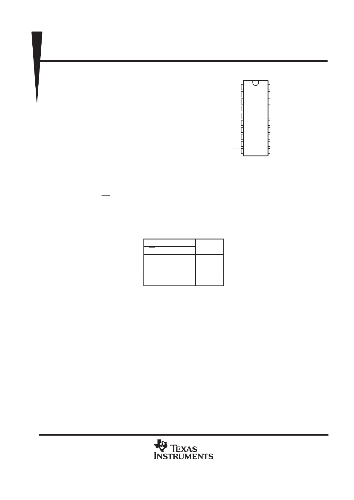
1Q
2Q
3Q
4Q
GND
5Q
6Q
7Q
8Q
OE
1D
2D
3D
4D
V
CC
5D
6D
7D
8D
CLK
DW OR N PACKAGE
(TOP VIEW)
PRODUCTION DATA information is current as of publication date.
Products conform to specifications per the terms of Texas Instruments
standard warranty. Production processing does not necessarily include
testing of all parameters.
SN74AS4374B
OCTAL EDGE-TRIGGERED D-TYPE DUAL-RANK FLIP-FLOP
WITH 3-STATE OUTPUTS
SDAS109D – APRIL 1989 – REVISED JANUARY 1995
2
POST OFFICE BOX 655303 • DALLAS, TEXAS 75265
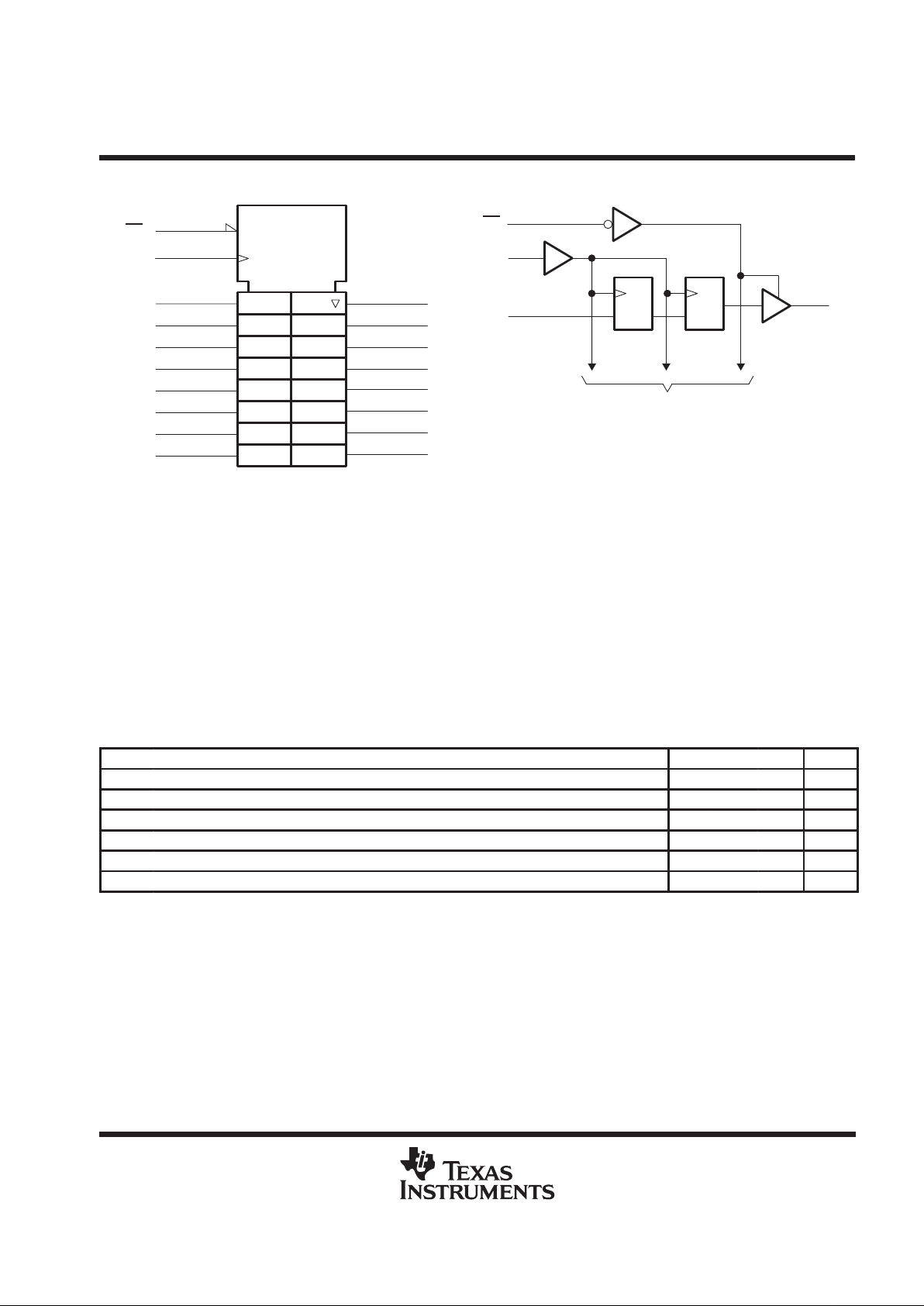
logic symbol
†
logic diagram (positive logic)
1D
CLK
1Q
1
11
20
10
1D
C1
OE
OE
EN
10
11
CLK
1D
20
1D
19
2D
18
3D
17
4D
5Q
6
6Q
7
7Q
8
8Q
9
15
5D
14
6D
13
7D
12
8D
1Q
1
2Q
2
3Q
3
4Q
4
C1
To Seven Other Channels
1D
1D
C1
†
This symbol is in accordance with ANSI/IEEE Std 91-1984
and IEC Publication 617-12.
absolute maximum ratings over operating free-air temperature range (unless otherwise noted)
‡
Supply voltage, V
CC
7 V. . . . . . . . . . . . . . . . . . . . . . . . . . . . . . . . . . . . . . . . . . . . . . . . . . . . . . . . . . . . . . . . . . . . . . . .
Input voltage, V
I
5.5 V. . . . . . . . . . . . . . . . . . . . . . . . . . . . . . . . . . . . . . . . . . . . . . . . . . . . . . . . . . . . . . . . . . . . . . . . . .
Voltage applied to any output in the high state or power-off state, V
O
5.5 V. . . . . . . . . . . . . . . . . . . . . . . . . . . .
Operating free-air temperature range, T
A
0°C to 70°C. . . . . . . . . . . . . . . . . . . . . . . . . . . . . . . . . . . . . . . . . . . . . .
Storage temperature range –65°C to 150°C. . . . . . . . . . . . . . . . . . . . . . . . . . . . . . . . . . . . . . . . . . . . . . . . . . . . . . .
‡
Stresses beyond those listed under “absolute maximum ratings” may cause permanent damage to the device. These are stress ratings only, and
functional operation of the device at these or any other conditions beyond those indicated under “recommended operating conditions” is not
implied. Exposure to absolute-maximum-rated conditions for extended periods may affect device reliability.
recommended operating conditions
MIN NOM MAX UNIT
V
CC
Supply voltage 4.5 5 5.5 V
V
IH
High-level input voltage 2 V
V
IL
Low-level input voltage 0.8 V
I
OH
High-level output current –15 mA
I
OL
Low-level output current 48 mA
T
A
Operating free-air temperature 0 70 °C
 Loading...