Texas Instruments SN74AS298AD, SN74AS298ADR, SN74AS298AN Datasheet

SN74AS298A
QUADRUPLE 2-INPUT MULTIPLEXER
WITH STORAGE
SDAS219B – DECEMBER 1983 – REVISED DECEMBER 1994
Copyright 1994, Texas Instruments Incorporated
1
POST OFFICE BOX 655303 • DALLAS, TEXAS 75265
• Selects One of Two 4-Bit Data Sources and
Synchronously Stores Data With System
Clock
• Applications:
– Dual Source for Operands and Constants
in Arithmetic Processor; Can Release
Processor Register Files for Acquiring
New Data
– Implements Separate Registers Capable
of Parallel Exchange of Contents, Yet
Retains External Load Capability
– Has Universal-Type Register for
Implementing Various Shift Patterns,
Including Compound Left-Right
Capability
• Package Options Include Plastic
Small-Outline (D) Packages and Standard
Plastic (N) 300-mil DIPs
description
The SN74AS298A is a quadruple 2-input multiplexer with storage that provides essentially the equivalent
functional capabilities of two separate MSI functions (SN74AS157 and ′AS175A) in a 16-pin package.
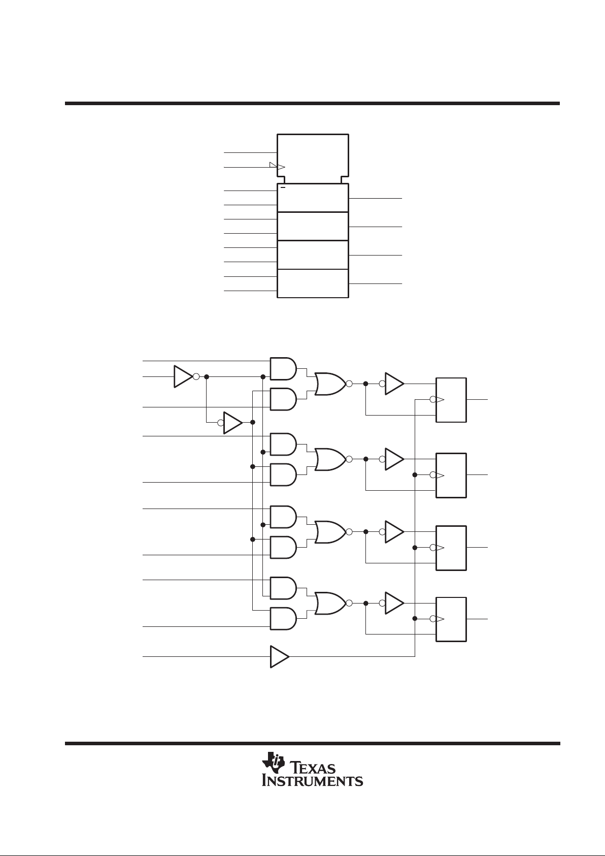
When the word-select (WS) input is low, word 1 (A1, B1, C1, D1) is applied to the flip-flops. A high input to WS
causes the selection of word 2 (A2, B2, C2, D2). The selected word is clocked to the output terminals on the
negative-going edge of the clock pulse.
The SN74AS298A is characterized for operation from 0°C to 70°C.
FUNCTION TABLE
INPUTS
OUTPUTS
†
WS CLK Q
A
Q
B
Q
C
Q
D
L ↓ a1 b1 c1 d1
H ↓ a2 b2 c2 d2
X H Q
A0QB0QC0QD0
†
a1, a2, etc. = the level of steady-state input at A1,
A2, etc.
QA0, QB0, etc. = the level of QA, QB, etc. entered
on the most recent ↓ transition of CLK
D OR N PACKAGE
(TOP VIEW)
1
2
3
4
5
6
7
8
16
15
14
13
12
11
10
9
B2
A2
A1
B1
C2
D2
D1
GND
V
CC
Q
A
Q
B
Q
C
Q
D
CLK
WS
C1
PRODUCTION DATA information is current as of publication date.
Products conform to specifications per the terms of Texas Instruments
standard warranty. Production processing does not necessarily include
testing of all parameters.

SN74AS298A
QUADRUPLE 2-INPUT MULTIPLEXER
WITH STORAGE
SDAS219B – DECEMBER 1983 – REVISED DECEMBER 1994
2
POST OFFICE BOX 655303 • DALLAS, TEXAS 75265
logic symbol
†
MUX
3
A1
1, 2D
2
A2
11
CLK
G1
10
WS
15
4
B1
1
B2
14
9
C1
5
C2
13
7
D1
6
D2
12
1, 2D
C2
Q
A
Q
B
Q
C
Q
D
†
This symbol is in accordance with ANSI/IEEE Std 91-1984 and IEC Publication 617-12.
logic diagram (positive logic)
Q
D
Q
C
Q
B
Q
A
D2
D1
C2
C1
B2
A2
A1
CLK
B1
WS
1S
C1
1S
C1
1S
C1
1S
C1
3
2
10
4
1
9
5
7
6
11
15
14
13
12
1R
1R
1R
1R

SN74AS298A
QUADRUPLE 2-INPUT MULTIPLEXER
WITH STORAGE
SDAS219B – DECEMBER 1983 – REVISED DECEMBER 1994
3
POST OFFICE BOX 655303 • DALLAS, TEXAS 75265
absolute maximum ratings over operating free-air temperature range (unless otherwise noted)
†
Supply voltage, V
CC
7 V. . . . . . . . . . . . . . . . . . . . . . . . . . . . . . . . . . . . . . . . . . . . . . . . . . . . . . . . . . . . . . . . . . . . . . . .
Input voltage, V
I
7 V. . . . . . . . . . . . . . . . . . . . . . . . . . . . . . . . . . . . . . . . . . . . . . . . . . . . . . . . . . . . . . . . . . . . . . . . . . . .
Operating free-air temperature range, T
A
0°C to 70°C. . . . . . . . . . . . . . . . . . . . . . . . . . . . . . . . . . . . . . . . . . . . . .
Storage temperature range 65°C to 150°C. . . . . . . . . . . . . . . . . . . . . . . . . . . . . . . . . . . . . . . . . . . . . . . . . . . . . . . . .
†
Stresses beyond those listed under “absolute maximum ratings” may cause permanent damage to the device. These are stress ratings only, and
functional operation of the device at these or any other conditions beyond those indicated under “recommended operating conditions” is not
implied. Exposure to absolute-maximum-rated conditions for extended periods may affect device reliability.
recommended operating conditions
MIN NOM MAX UNIT
V
CC
Supply voltage 4.5 5 5.5 V
V
IH
High-level input voltage 2 V
V
IL
Low-level input voltage 0.8 V
I
OH
High-level output current –2 mA
I
OL
Low-level output current 20 mA
T
A
Operating free-air temperature 0 70 °C
electrical characteristics over recommended operating free-air temperature range (unless
otherwise noted)
PARAMETER TEST CONDITIONS MIN TYP‡MAX UNIT
V
IK
VCC = 4.5 V, II = –18 mA –1.2 V
V
OH
VCC = 4.5 V to 5.5 V, IOH = –2 mA VCC–2 V
V
OL
VCC = 4.5 V, IOL = 20 mA 0.35 0.5 V
I
I
VCC = 5.5 V, VI = 7 V 0.1 mA
WS
40
I
IH
All others
V
CC
= 5.5 V,
V
I
= 2.7
V
20
µ
A
WS
–0.75
I
IL
All others
V
CC
=
5.5 V
,
V
I
=
0.4 V
–0.5
mA
I
O
§
VCC = 5.5 V, VO = 2.25 V –30 –112 mA
I
CCH
VCC = 5.5 V 21 33 mA
I
CCL
VCC = 5.5 V 22 36 mA
‡
All typical values are at VCC = 5 V, TA = 25°C.
§
The output conditions have been chosen to produce a current that closely approximates one half of the true short-circuit output current, IOS.
timing requirements over recommended operating free-air temperature range (unless otherwise
noted)
MIN MAX UNIT
f
clock
Clock frequency 0 62 MHz
t
w
Pulse duration, CLK high or low 8 ns
p
Data 4.5
tsuSetup time before CLK↓
WS 13
ns
Data 3.5
thHold time after CLK↓
WS 1
ns
 Loading...