


SN74AS1804
HEX 2-INPUT NAND DRIVER
SDAS042C – AUGUST 1984 – REVISED JANUAR Y 1995
• High Capacitive-Drive Capability
• Typical Delay Time of 2.6 ns (C
and Typical Power Dissipation of Less
Than 9 mW Per Gate
• Center V
and GND Configuration
CC
Provides Minimum Lead Inductance in
High-Current Switching Applications
• Package Options Include Plastic
Small-Outline (DW) Packages and Standard
Plastic (N) 300-mil DIPs
description
= 50 pF)
L
DW OR N PACKAGE
(TOP VIEW)
5B
1
20
6Y
2
19
6A
3
18
6B
4
17
V
5
6
7
8
9
10
16
15
14
13
12
11
CC
1A
1B
1Y
2A
2B
5A
5Y
4B
4A
4Y
GND
3Y
3B
3A
2Y
This device contains six independent 2-input
NAND drivers. It performs the Boolean functions
Y = A
• B or Y = A + B in positive logic.
The center-pin configuration reduces lead inductance when compared to the ′AS804B. The reduced lead
inductance minimizes noise generated onto either the V
or GND bus. This reduction is significant in
CC
high-current switching applications.
The SN74AS1804 is characterized for operation from 0°C to 70°C.
FUNCTION TABLE
(each driver)
INPUTS
A B
H H L
L XH
XLH
OUTPUT
Y
6
7
9
10
12
13
17
18
20
1
3
4
†
&
8
11
14
16
19
2
logic symbol
1A
1B
2A
2B
3A
3B
4A
4B
5A
5B
6A
6B
†
This symbol is in accordance with ANSI/IEEE Std 91-1984 and
IEC Publication 617-12.
PRODUCTION DATA information is current as of publication date.
Products conform to specifications per the terms of Texas Instruments
standard warranty. Production processing does not necessarily include
testing of all parameters.
logic diagram (positive logic)
6
1Y
2Y
3Y
4Y
5Y
6Y
1A
1B
2A
2B
3A
3B
4A
4B
5A
5B
6A
6B
7
9
10
12
13
17
18
20
1
3
4
8
1Y
11
2Y
14
3Y
16
4Y
19
5Y
2
6Y
Copyright 1995, Texas Instruments Incorporated
POST OFFICE BOX 655303 • DALLAS, TEXAS 75265
1
SN74AS1804
V
4.5 V
A or B
Y
ns
HEX 2-INPUT NAND DRIVER
SDAS042C – AUGUST 1984 – REVISED JANUAR Y 1995
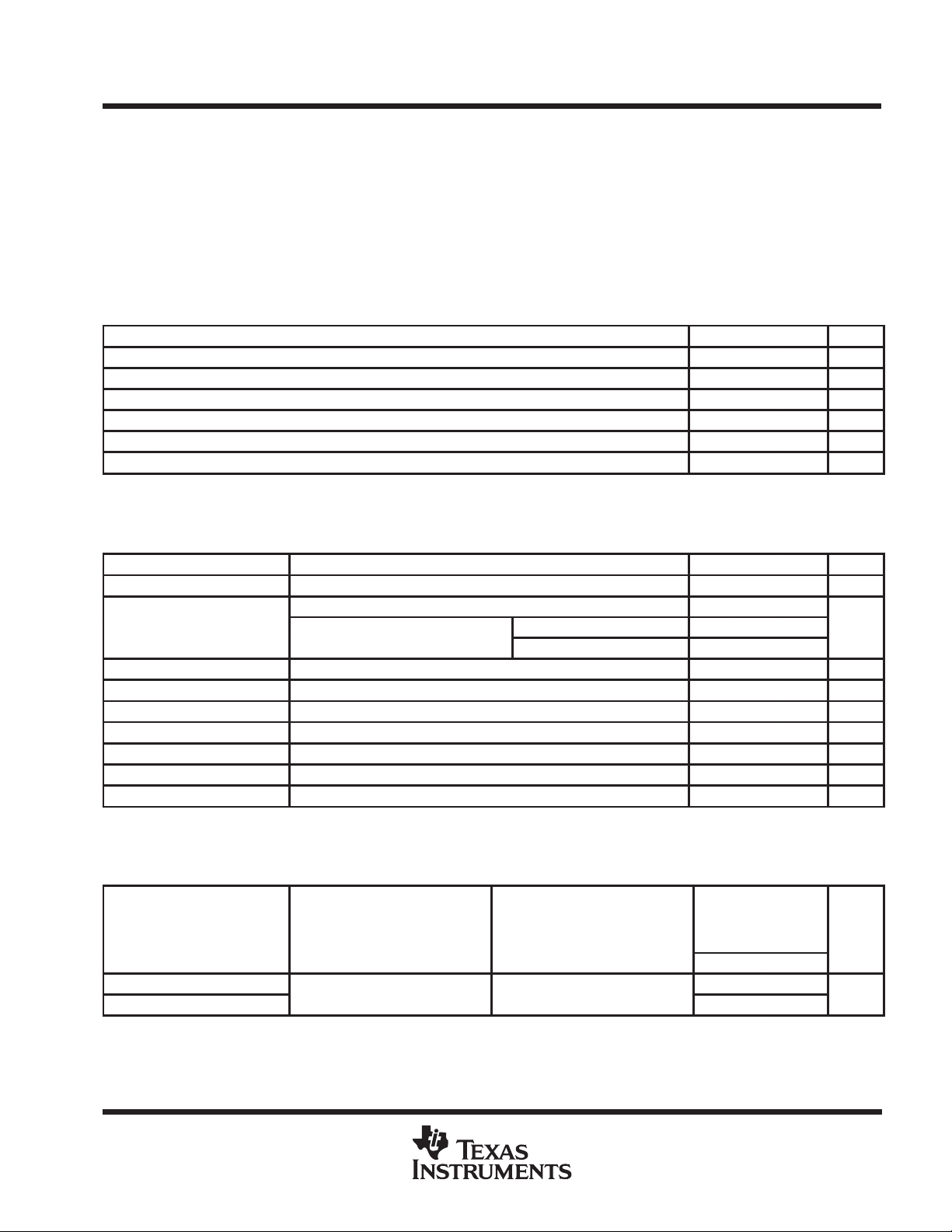
absolute maximum ratings over operating free-air temperature range (unless otherwise noted)
Supply voltage, V
Input voltage, V
Operating free-air temperature range, T
7 V. . . . . . . . . . . . . . . . . . . . . . . . . . . . . . . . . . . . . . . . . . . . . . . . . . . . . . . . . . . . . . . . . . . . . . . .
CC
7 V. . . . . . . . . . . . . . . . . . . . . . . . . . . . . . . . . . . . . . . . . . . . . . . . . . . . . . . . . . . . . . . . . . . . . . . . . . . .
I
0°C to 70°C. . . . . . . . . . . . . . . . . . . . . . . . . . . . . . . . . . . . . . . . . . . . . .
A
†
Storage temperature range –65°C to 150°C. . . . . . . . . . . . . . . . . . . . . . . . . . . . . . . . . . . . . . . . . . . . . . . . . . . . . . .
†
Stresses beyond those listed under “absolute maximum ratings” may cause permanent damage to the device. These are stress ratings only, and
functional operation of the device at these or any other conditions beyond those indicated under “recommended operating conditions” is not
implied. Exposure to absolute-maximum-rated conditions for extended periods may affect device reliability.
recommended operating conditions
V
CC
V
IH
V
IL
I
OH
I
OL
T
A
‡
This high sink- or source-current device is not recommended for use above 40 MHz.
Supply voltage 4.5 5 5.5 V
High-level input voltage 2 V
Low-level input voltage 0.8 V
High-level output current –48 mA
Low-level output current 48 mA
Operating free-air temperature 0 70 °C
‡
MIN NOM MAX UNIT
electrical characteristics over recommended operating free-air temperature range (unless
otherwise noted)
PARAMETER TEST CONDITIONS MIN TYP§MAX UNIT
V
IK
V
OH
V
OL
I
I
I
IH
I
IL
¶
I
O
I
CCH
I
§
All typical values are at VCC = 5 V, TA = 25°C.
¶
The output conditions have been chosen to produce a current that closely approximates one half of the true short-circuit output current, IOS.
CCL
VCC = 4.5 V, II = –18 mA –1.2 V
VCC = 4.5 V to 5.5 V, IOH = –2 mA VCC –2
=
CC
VCC = 4.5 V, IOL = 48 mA 0.35 0.5 V
VCC = 5.5 V, VI = 7 V 0.1 mA
VCC = 5.5 V, VI = 2.7 V 20 µA
VCC = 5.5 V, VI = 0.4 V –0.5 mA
VCC = 5.5 V, VO = 2.25 V –50 –200 mA
VCC = 5.5 V, VI = 0 3.5 5 mA
VCC = 5.5 V, VI = 4.5 V 16 27 mA
IOH = –3 mA 2.4 3.2
IOH = –48 mA 2
V
switching characteristics (see Figure 1)
PARAMETER
t
PLH
t
#
For conditions shown as MIN or MAX, use the appropriate value specified under recommended operating conditions.
2
PHL
FROM
(INPUT)
POST OFFICE BOX 655303 • DALLAS, TEXAS 75265
TO
(OUTPUT)
VCC = 4.5 V to 5.5 V,
CL = 50 pF,
RL = 500 Ω,
TA = MIN to MAX
MIN MAX
1 4
1 4
#
UNIT
 Loading...