

SN54ALVTH32373, SN74ALVTH32373
2.5-V/3.3-V 32-BIT TRANSPARENT D-TYPE LATCHES
WITH 3-STATE OUTPUTS
SCES322A – FEBRUARY 2000 – REVISED APRIL 2000
1
POST OFFICE BOX 655303 • DALLAS, TEXAS 75265
D
State-of-the-Art Advanced BiCMOS
Technology (ABT)
Widebus+
Design for
2.5-V and 3.3-V Operation and Low
Static-Power Dissipation
D
Support Mixed-Mode Signal Operation (5-V
Input and Output Voltages With 2.3-V to
3.6-V V
CC
)
D
T ypical V
OLP
(Output Ground Bounce)
<0.8 V at VCC = 3.3 V, TA = 25°C
D
High Drive (–24/24 mA at 2.5-V and
–32/64 mA at 3.3-V VCC)
D
I
off
and Power-Up 3-State Support Hot
Insertion
D
Use Bus Hold on Data Inputs in Place of
External Pullup/Pulldown Resistors to
Prevent the Bus From Floating
NOTE: For tape and reel order entry:
The GKER package is abbreviated to KR.
D
Auto3-State Eliminates Bus Current
Loading When Output Exceeds VCC + 0.5 V
D
Flow-Through Architecture Facilitates
Printed Circuit Board Layout
D
Distributed VCC and GND Pins Minimize
High-Speed Switching Noise
D
Latch-Up Performance Exceeds 100 mA Per
JESD 78, Class II
D
ESD Protection Exceeds JESD 22
– 2000-V Human-Body Model (A114-A)
– 200-V Machine Model (A115-A)
– 1000-V Charged-Device Model (C101)
D
Packaged in Plastic Fine-Pitch Ball Grid
Array Package
description
The ’AL VTH32373 devices are 32-bit transparent D-type latches with 3-state outputs designed for 2.5-V or 3.3-V
V
CC
operation, but with the capability to provide a TTL interface to a 5-V system environment. These devices
are particularly suitable for implementing buffer registers, I/O ports, bidirectional bus drivers, and working
registers.
These devices can be used as four 8-bit latches, two 16-bit latches, or one 32-bit latch. When the latch-enable
(LE) input is high, the Q outputs follow the data (D) inputs. When LE is taken low, the Q outputs are latched at
the levels set up at the D inputs.
A buffered output-enable (OE) input can be used to place the eight outputs in either a normal logic state (high
or low logic levels) or the high-impedance state. In the high-impedance state, the outputs neither load nor drive
the bus lines significantly . The high-impedance state and increased drive provide the capability to drive bus lines
without interface or pullup components.
OE does not affect internal operations of the latch. Old data can be retained or new data can be entered while
the outputs are in the high-impedance state.
Inputs can be driven from either 3.3-V or 5-V devices. This feature allows the use of these devices as translators
in a mixed 3.3-V/5-V system environment.
These devices are fully specified for hot-insertion applications using I
off
and power-up 3-state. The I
off
circuitry
disables the outputs, preventing damaging current backflow through the devices when they are powered down.
The power-up 3-state circuitry places the outputs in the high-impedance state during power up and power down,
which prevents driver conflict.
When V
CC
is between 0 and 1.2 V , the devices are in the high-impedance state during power up or power down.
However, to ensure the high-impedance state above 1.2 V, OE should be tied to VCC through a pullup resistor;
the minimum value of the resistor is determined by the current-sinking capability of the driver.
Copyright 2000, Texas Instruments Incorporated
Please be aware that an important notice concerning availability, standard warranty, and use in critical applications of
Texas Instruments semiconductor products and disclaimers thereto appears at the end of this data sheet.
Widebus+ is a trademark of Texas Instruments.
UNLESS OTHERWISE NOTED this document contains PRODUCTION
DATA information current as of publication date. Products conform to
specifications per the terms of Texas Instruments standard warranty.
Production processing does not necessarily include testing of all
parameters.
SN54ALVTH32373, SN74ALVTH32373
2.5-V/3.3-V 32-BIT TRANSPARENT D-TYPE LATCHES
WITH 3-STATE OUTPUTS
SCES322A – FEBRUARY 2000 – REVISED APRIL 2000
2
POST OFFICE BOX 655303 • DALLAS, TEXAS 75265
description (continued)
Active bus-hold circuitry is provided to hold unused or floating data inputs at a valid logic level.
The SN54ALVTH32373 is characterized for operation over the full military temperature range of –55°C to
125°C. The SN74ALVTH32373 is characterized for operation from –40°C to 85°C.
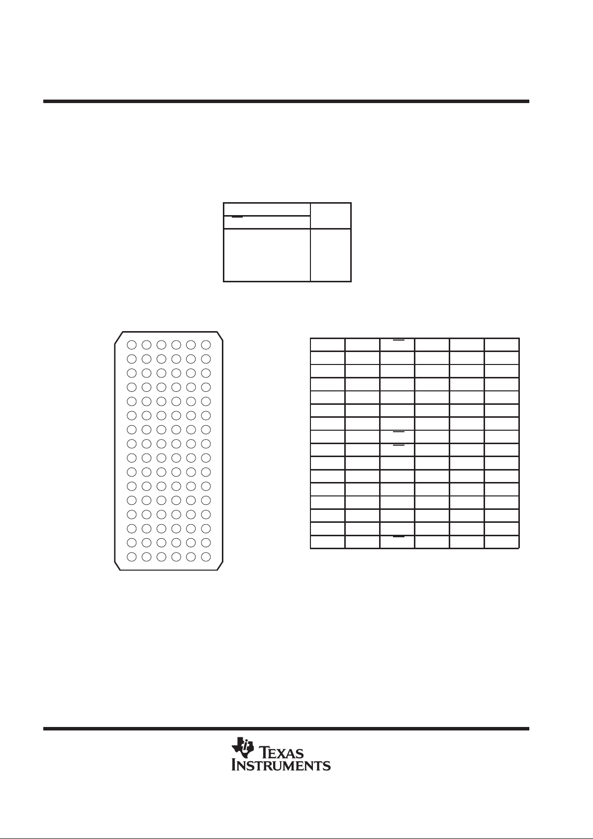
FUNCTION TABLE
(each 8-bit latch)
INPUTS
OUTPUT
OE LE D
Q
L H H H
L HL L
L LX Q
0
H X X Z
terminal assignments
123456
A 1Q2
1Q1 1OE 1LE 1D1 1D2
B 1Q4 1Q3 GND GND 1D3 1D4
C 1Q6 1Q5 1V
CC
1V
CC
1D5 1D6
D 1Q8 1Q7 GND GND 1D7 1D8
E 2Q2 2Q1 GND GND 2D1 2D2
F 2Q4 2Q3 1V
CC
1V
CC
2D3 2D4
G 2Q6 2Q5 GND GND 2D5 2D6
H 2Q7 2Q8 2OE 2LE 2D8 2D7
J 3Q2 3Q1 3OE 3LE 3D1 3D2
K 3Q4 3Q3 GND GND 3D3 3D4
L 3Q6 3Q5 2V
CC
2V
CC
3D5 3D6
M 3Q8 3Q7 GND GND 3D7 3D8
N 4Q2 4Q1 GND GND 4D1 4D2
P 4Q4 4Q3 2V
CC
2V
CC
4D3 4D4
R 4Q6 4Q5 GND GND 4D5 4D6
T 4Q7 4Q8 4OE 4LE 4D8 4D7
GKE PACKAGE
(TOP VIEW)
123456
A
B
C
D
E
F
G
H
J
K
L
M
N
P
R
T
SN54ALVTH32373, SN74ALVTH32373
2.5-V/3.3-V 32-BIT TRANSPARENT D-TYPE LATCHES
WITH 3-STATE OUTPUTS
SCES322A – FEBRUARY 2000 – REVISED APRIL 2000
3
POST OFFICE BOX 655303 • DALLAS, TEXAS 75265
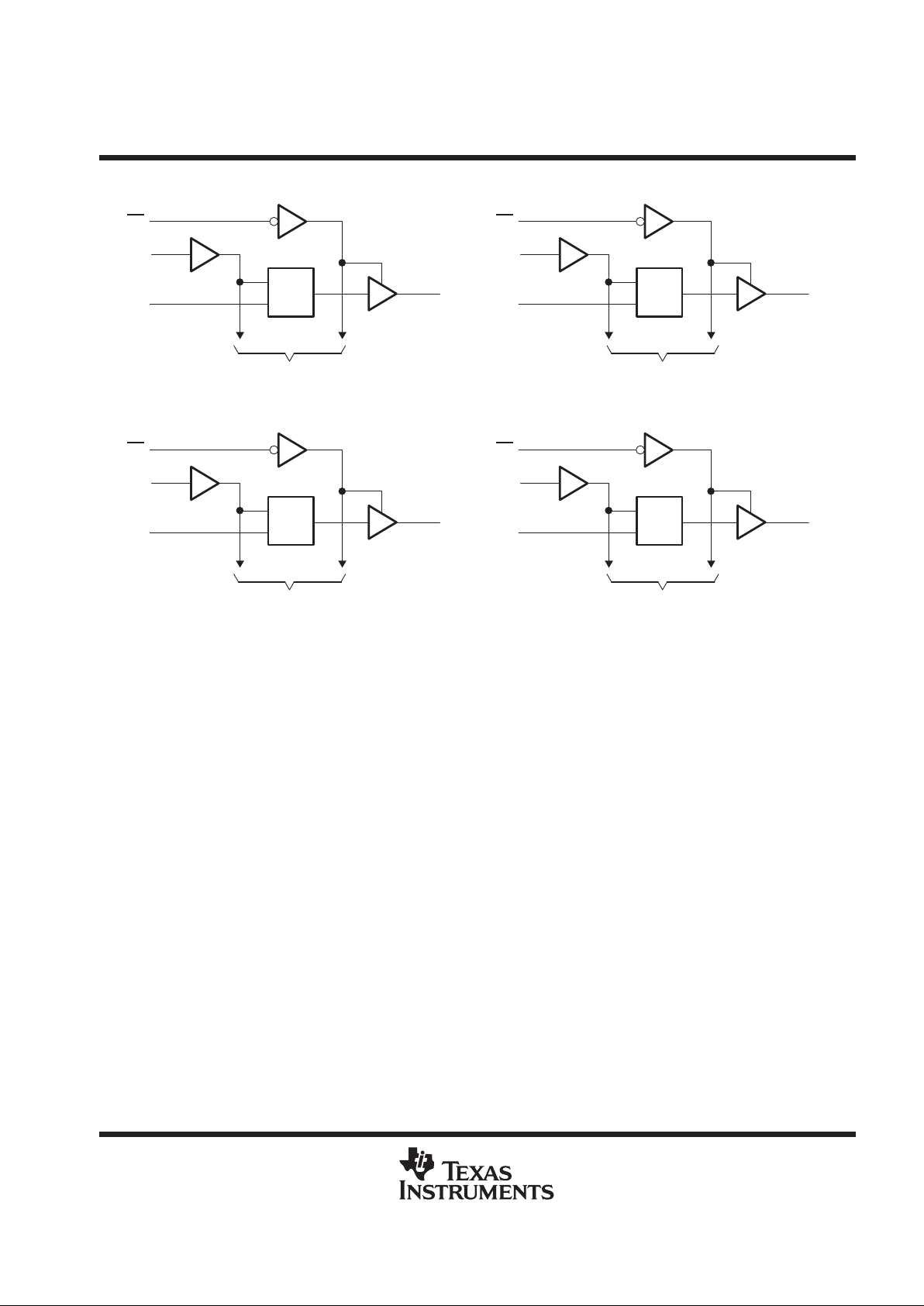
logic diagram (positive logic)
1OE
1LE
1D1
To Seven Other Channels
1Q1
C1
1D
A3
A4
A5
A2
2OE
2LE
2D1
To Seven Other Channels
2Q1
C1
1D
H3
H4
E5
E2
3OE
3LE
3D1
To Seven Other Channels
3Q1
C1
1D
J3
J4
J5
J2
4OE
4LE
4D1
To Seven Other Channels
4Q1
C1
1D
T3
T4
N5
N2
NOTE A: 1VCC is associated with these channels.
NOTE B: 2VCC is associated with these channels.
absolute maximum ratings over operating free-air temperature range (unless otherwise noted)
†
Supply voltage range, VCC –0.5 V to 4.6 V. . . . . . . . . . . . . . . . . . . . . . . . . . . . . . . . . . . . . . . . . . . . . . . . . . . . . . . . .
Input voltage range, V
I
(see Note 1) –0.5 V to 7 V. . . . . . . . . . . . . . . . . . . . . . . . . . . . . . . . . . . . . . . . . . . . . . . . . .
Voltage range applied to any output in the high-impedance
or power-off state, VO (see Note 1) –0.5 V to 7 V. . . . . . . . . . . . . . . . . . . . . . . . . . . . . . . . . . . . . . . . . . . . . . . .
Voltage range applied to any output in the high state, VO (see Note 1) –0.5 V to 7 V. . . . . . . . . . . . . . . . . . . .
Output current in the low state, IO: SN54ALVTH32373 96 mA. . . . . . . . . . . . . . . . . . . . . . . . . . . . . . . . . . . . . . . .
SN74ALVTH32373 128 mA. . . . . . . . . . . . . . . . . . . . . . . . . . . . . . . . . . . . . . .
Output current in the high state, I
O
: SN54ALVTH32373 –48 mA. . . . . . . . . . . . . . . . . . . . . . . . . . . . . . . . . . . . . .
SN74ALVTH32373 –64 mA. . . . . . . . . . . . . . . . . . . . . . . . . . . . . . . . . . . . . .
Continuous current through VCC or GND ±100 mA. . . . . . . . . . . . . . . . . . . . . . . . . . . . . . . . . . . . . . . . . . . . . . . . . .
Input clamp current, I
IK
(V
I
< 0) –50 mA. . . . . . . . . . . . . . . . . . . . . . . . . . . . . . . . . . . . . . . . . . . . . . . . . . . . . . . . . . .
Output clamp current, I
OK
(V
O
< 0) –50 mA. . . . . . . . . . . . . . . . . . . . . . . . . . . . . . . . . . . . . . . . . . . . . . . . . . . . . . . .
Package thermal impedance, θ
JA
(see Note 2) 40°C/W. . . . . . . . . . . . . . . . . . . . . . . . . . . . . . . . . . . . . . . . . . . . .
Storage temperature range, T
stg
–65°C to 150°C. . . . . . . . . . . . . . . . . . . . . . . . . . . . . . . . . . . . . . . . . . . . . . . . . . .
†
Stresses beyond those listed under “absolute maximum ratings” may cause permanent damage to the device. These are stress ratings only, and
functional operation of the device at these or any other conditions beyond those indicated under “recommended operating conditions” is not
implied. Exposure to absolute-maximum-rated conditions for extended periods may affect device reliability.
NOTES: 1. The input and output negative-voltage ratings may be exceeded if the input and output clamp-current ratings are observed.
2. The package thermal impedance is calculated in accordance with JESD 51.

SN54ALVTH32373, SN74ALVTH32373
2.5-V/3.3-V 32-BIT TRANSPARENT D-TYPE LATCHES
WITH 3-STATE OUTPUTS
SCES322A – FEBRUARY 2000 – REVISED APRIL 2000
4
POST OFFICE BOX 655303 • DALLAS, TEXAS 75265
recommended operating conditions, VCC = 2.5 V ± 0.2 V (see Note 3)
SN54ALVTH32373 SN74ALVTH32373
MIN TYP MAX MIN TYP MAX
UNIT
V
CC
Supply voltage 2.3 2.7 2.3 2.7 V
V
IH
High-level input voltage 1.7 1.7 V
V
IL
Low-level input voltage 0.7 0.7 V
V
I
Input voltage 0 V
CC
5.5 0 V
CC
5.5 V
I
OH
High-level output current –6 –8 mA
Low-level output current 6 8
I
OL
Low-level output current; current duty cycle ≤ 50%; f ≥ 1 kHz 18 24
mA
∆t/∆v Input transition rise or fall rate Outputs enabled 10 10 ns/V
∆t/∆V
CC
Power-up ramp rate 200 200 µs/V
T
A
Operating free-air temperature –55 125 –40 85 °C
NOTE 3: All unused control inputs of the device must be held at VCC or GND to ensure proper device operation. Refer to the TI application report,
Implications of Slow or Floating CMOS Inputs
, literature number SCBA004.
recommended operating conditions, VCC = 3.3 V ± 0.3 V (see Note 3)
SN54ALVTH32373 SN74ALVTH32373
MIN TYP MAX MIN TYP MAX
UNIT
V
CC
Supply voltage 3 3.6 3 3.6 V
V
IH
High-level input voltage 2 2 V
V
IL
Low-level input voltage 0.8 0.8 V
V
I
Input voltage 0 V
CC
5.5 0 V
CC
5.5 V
I
OH
High-level output current –24 –32 mA
Low-level output current 24 32
I
OL
Low-level output current; current duty cycle ≤ 50%; f ≥ 1 kHz 48 64
mA
∆t/∆v Input transition rise or fall rate Outputs enabled 10 10 ns/V
∆t/∆V
CC
Power-up ramp rate 200 200 µs/V
T
A
Operating free-air temperature –55 125 –40 85 °C
NOTE 3: All unused control inputs of the device must be held at VCC or GND to ensure proper device operation. Refer to the TI application report,
Implications of Slow or Floating CMOS Inputs
, literature number SCBA004.
PRODUCT PREVIEW information concerns products in the formative or
design phase of development. Characteristic data and other
specifications are design goals. Texas Instruments reserves the right to
change or discontinue these products without notice.

SN54ALVTH32373, SN74ALVTH32373
2.5-V/3.3-V 32-BIT TRANSPARENT D-TYPE LATCHES
WITH 3-STATE OUTPUTS
SCES322A – FEBRUARY 2000 – REVISED APRIL 2000
5
POST OFFICE BOX 655303 • DALLAS, TEXAS 75265
electrical characteristics over recommended operating free-air temperature range,
V
CC
= 2.5 V ± 0.2 V (unless otherwise noted)
SN54ALVTH32373 SN74ALVTH32373
PARAMETER
TEST CONDITIONS
MIN TYP†MAX MIN TYP†MAX
UNIT
V
IK
VCC = 2.3 V, II = –18 mA –1.2 –1.2 V
VCC = 2.3 V to 2.7 V, IOH = –100 µA VCC–0.2 VCC–0.2
V
OH
IOH = –6 mA 1.8
V
V
CC
= 2.3
V
IOH = –8 mA 1.8
VCC = 2.3 V to 2.7 V, IOL = 100 µA 0.2 0.2
IOL = 6 mA 0.4
V
OL
IOL = 8 mA 0.4
V
V
CC
= 2.3
V
IOL = 18 mA 0.5
IOL = 24 mA 0.5
p
VCC = 2.7 V, VI = VCC or GND ±1 ±1
Control inputs
VCC = 0 or 2.7 V, VI = 5.5 V 10 10
I
I
VI = 5.5 V 10 10
µA
Data inputs VCC = 2.7 V
VI = V
CC
1 1
VI = 0 –5 –5
I
off
VCC = 0, VI or VO = 0 to 4.5 V ±100 µA
I
BHL
‡
VCC = 2.3 V, VI = 0.7 V 115* 115 µA
I
BHH
§
VCC = 2.3 V, VI = 1.7 V –10* –10 µA
I
BHLO
¶
VCC = 2.7 V, VI = 0 to V
CC
300* 300 µA
I
BHHO
#
VCC = 2.7 V, VI = 0 to V
CC
–300* –300 µA
I
EX
||
VCC = 2.3 V, VO = 5.5 V 125 125 µA
I
OZ(PU/PD)
k
VCC ≤ 1.2 V, VO = 0.5 V to VCC,
VI = GND or VCC, OE
= don’t care
±100 ±100 µA
I
OZH
VCC = 2.7 V
VO = 2.3 V,
VI = 0.7 V or 1.7 V
5 5 µA
I
OZL
VCC = 2.7 V
VO = 0.5 V,
VI = 0.7 V or 1.7 V
–5 –5 µA
=
Outputs high 0.04 0.1 0.04 0.1
I
CC
V
CC
= 2.7 V,
IO = 0,
Outputs low 2.3 4.5 2.3 4.5
mA
VI = VCC or GND
Outputs disabled 0.04 0.1 0.04 0.1
C
i
VCC = 2.5 V, VI = 2.5 V or 0 3.5 3.5 pF
C
o
VCC = 2.5 V, VO = 2.5 V or 0 6 6 pF
* On products compliant to MIL-PRF-38535, this parameter is not production tested.
†
All typical values are at VCC = 2.5 V, TA = 25°C.
‡
The bus-hold circuit can sink at least the minimum low sustaining current at VIL max. I
BHL
should be measured after lowering VIN to GND and
then raising it to VIL max.
§
The bus-hold circuit can source at least the minimum high sustaining current at VIH min. I
BHH
should be measured after raising VIN to VCC and
then lowering it to VIH min.
¶
An external driver must source at least I
BHLO
to switch this node from low to high.
#
An external driver must sink at least I
BHHO
to switch this node from high to low.
||
Current into an output in the high state when VO > V
CC
k
High-impedance state during power up or power down
PRODUCT PREVIEW information concerns products in the formative or
design phase of development. Characteristic data and other
specifications are design goals. Texas Instruments reserves the right to
change or discontinue these products without notice.

SN54ALVTH32373, SN74ALVTH32373
2.5-V/3.3-V 32-BIT TRANSPARENT D-TYPE LATCHES
WITH 3-STATE OUTPUTS
SCES322A – FEBRUARY 2000 – REVISED APRIL 2000
6
POST OFFICE BOX 655303 • DALLAS, TEXAS 75265
electrical characteristics over recommended operating free-air temperature range,
V
CC
= 3.3 V ± 0.3 V (unless otherwise noted)
SN54ALVTH32373 SN74ALVTH32373
PARAMETER
TEST CONDITIONS
MIN TYP†MAX MIN TYP†MAX
UNIT
V
IK
VCC = 3 V, II = –18 mA –1.2 –1.2 V
VCC = 3 V to 3.6 V, IOH = –100 µA VCC–0.2 VCC–0.2
V
OH
IOH = –24 mA 2
V
V
CC
= 3
V
IOH = –32 mA 2
VCC = 3 V to 3.6 V, IOL = 100 µA 0.2 0.2
IOL = 16 mA 0.4
IOL = 24 mA 0.5
V
OL
VCC = 3 V
IOL = 32 mA 0.5
V
IOL = 48 mA 0.55
IOL = 64 mA 0.55
p
VCC = 3.6 V, VI = VCC or GND ±1 ±1
Control inputs
VCC = 0 or 3.6 V, VI = 5.5 V 10 10
I
I
VI = 5.5 V 10 10
µA
Data inputs VCC = 3.6 V
VI = V
CC
1 1
VI = 0 –5 –5
I
off
VCC = 0, VI or VO = 0 to 4.5 V ±100 µA
I
BHL
‡
VCC = 3 V, VI = 0.8 V 75* 75 µA
I
BHH
§
VCC = 3 V, VI = 2 V –75* –75 µA
I
BHLO
¶
VCC = 3.6 V, VI = 0 to V
CC
500* 500 µA
I
BHHO
#
VCC = 3.6 V, VI = 0 to V
CC
–500* –500 µA
I
EX
||
VCC = 3 V, VO = 5.5 V 125 125 µA
I
OZ(PU/PD)
k
VCC ≤ 1.2 V, VO = 0.5 V to VCC,
VI = GND or VCC, OE
= don’t care
±100 ±100 µA
I
OZH
VCC = 3.6 V
VO = 3 V,
VI = 0.8 V or 2 V
5 5 µA
I
OZL
VCC = 3.6 V
VO = 0.5 V,
VI = 0.8 V or 2 V
–5 –5 µA
=
Outputs high 0.07 0.1 0.07 0.1
I
CC
V
CC
= 3.6 V,
IO = 0,
Outputs low 3.2 5 3.2 5
mA
VI = VCC or GND
Outputs disabled 0.07 0.1 0.07 0.1
∆I
CC
h
VCC = 3 V to 3.6 V, One input at VCC – 0.6 V,
Other inputs at VCC or GND
0.4 0.4 mA
C
i
VCC = 3.3 V, VI = 3.3 V or 0 3.5 3.5 pF
C
o
VCC = 3.3 V, VO = 3.3 V or 0 6 6 pF
* On products compliant to MIL-PRF-38535, this parameter is not production tested.
†
All typical values are at VCC = 3.3 V, TA = 25°C.
‡
The bus-hold circuit can sink at least the minimum low sustaining current at VIL max. I
BHL
should be measured after lowering VIN to GND and
then raising it to VIL max.
§
The bus-hold circuit can source at least the minimum high sustaining current at VIH min. I
BHH
should be measured after raising VIN to VCC and
then lowering it to VIH min.
¶
An external driver must source at least I
BHLO
to switch this node from low to high.
#
An external driver must sink at least I
BHHO
to switch this node from high to low.
||
Current into an output in the high state when VO > V
CC
k
High-impedance state during power up or power down
h
This is the increase in supply current for each input that is at the specified TTL voltage level rather than VCC or GND.
PRODUCT PREVIEW information concerns products in the formative or
design phase of development. Characteristic data and other
specifications are design goals. Texas Instruments reserves the right to
change or discontinue these products without notice.

SN54ALVTH32373, SN74ALVTH32373
2.5-V/3.3-V 32-BIT TRANSPARENT D-TYPE LATCHES
WITH 3-STATE OUTPUTS
SCES322A – FEBRUARY 2000 – REVISED APRIL 2000
7
POST OFFICE BOX 655303 • DALLAS, TEXAS 75265
timing requirements over recommended operating free-air temperature range, VCC = 2.5 V ± 0.2 V
(unless otherwise noted) (see Figure 1)
SN54ALVTH32373 SN74ALVTH32373
MIN MAX MIN MAX
UNIT
t
w
Pulse duration, LE high 1.5 1.5 ns
Data high 1.1 1
t
su
Set
up time, data before
LE↓
Data low 1.6 1.5
ns
Data high 1 0.9
t
h
Hold time, data after LE↓
Data low 1.6 1.5
ns
timing requirements over recommended operating free-air temperature range, VCC = 3.3 V ± 0.3 V
(unless otherwise noted) (see Figure 2)
SN54ALVTH32373 SN74ALVTH32373
MIN MAX MIN MAX
UNIT
t
w
Pulse duration, LE high 1.5 1.5 ns
Data high 1.5 1.4
t
su
Set
up time, data before
LE↓
Data low 1 0.9
ns
Data high 1 0.9
t
h
Hold time, data after LE↓
Data low 1.5 1.4
ns
switching characteristics over recommended operating free-air temperature range, CL = 30 pF,
V
CC
= 2.5 V ± 0.2 V (unless otherwise noted) (see Figure 1)
FROM TO
SN54ALVTH32373 SN74ALVTH32373
PARAMETER
(INPUT) (OUTPUT)
MIN MAX MIN MAX
UNIT
t
PLH
1 3.4 1 3.3
t
PHL
D
Q
1 4.3 1 4.2
ns
t
PLH
1.4 3.9 1.5 3.8
t
PHL
LE
Q
1.4 4.6 1.5 4.5
ns
t
PZH
1.7 4.4 1.8 4.3
t
PZL
OE
Q
1.4 4.1 1.5 4
ns
t
PHZ
1.4 4.7 1.5 4.6
t
PLZ
OE
Q
1 3.7 1 3.6
ns
switching characteristics over recommended operating free-air temperature range, CL = 50 pF,
V
CC
= 3.3 V ± 0.3 V (unless otherwise noted) (see Figure 2)
FROM TO
SN54ALVTH32373 SN74ALVTH32373
PARAMETER
(INPUT) (OUTPUT)
MIN MAX MIN MAX
UNIT
t
PLH
1 3.2 1 3.1
t
PHL
D
Q
1 3.4 1 3.3
ns
t
PLH
1 3.4 1 3.3
t
PHL
LE
Q
1 3.6 1 3.5
ns
t
PZH
1.3 4.1 1.4 4
t
PZL
OE
Q
1 3.5 1 3.4
ns
t
PHZ
1.4 5 1.5 4.9
t
PLZ
OE
Q
1.4 4.6 1.5 4.5
ns
PRODUCT PREVIEW information concerns products in the formative or
design phase of development. Characteristic data and other
specifications are design goals. Texas Instruments reserves the right to
change or discontinue these products without notice.
SN54ALVTH32373, SN74ALVTH32373
2.5-V/3.3-V 32-BIT TRANSPARENT D-TYPE LATCHES
WITH 3-STATE OUTPUTS
SCES322A – FEBRUARY 2000 – REVISED APRIL 2000
8
POST OFFICE BOX 655303 • DALLAS, TEXAS 75265
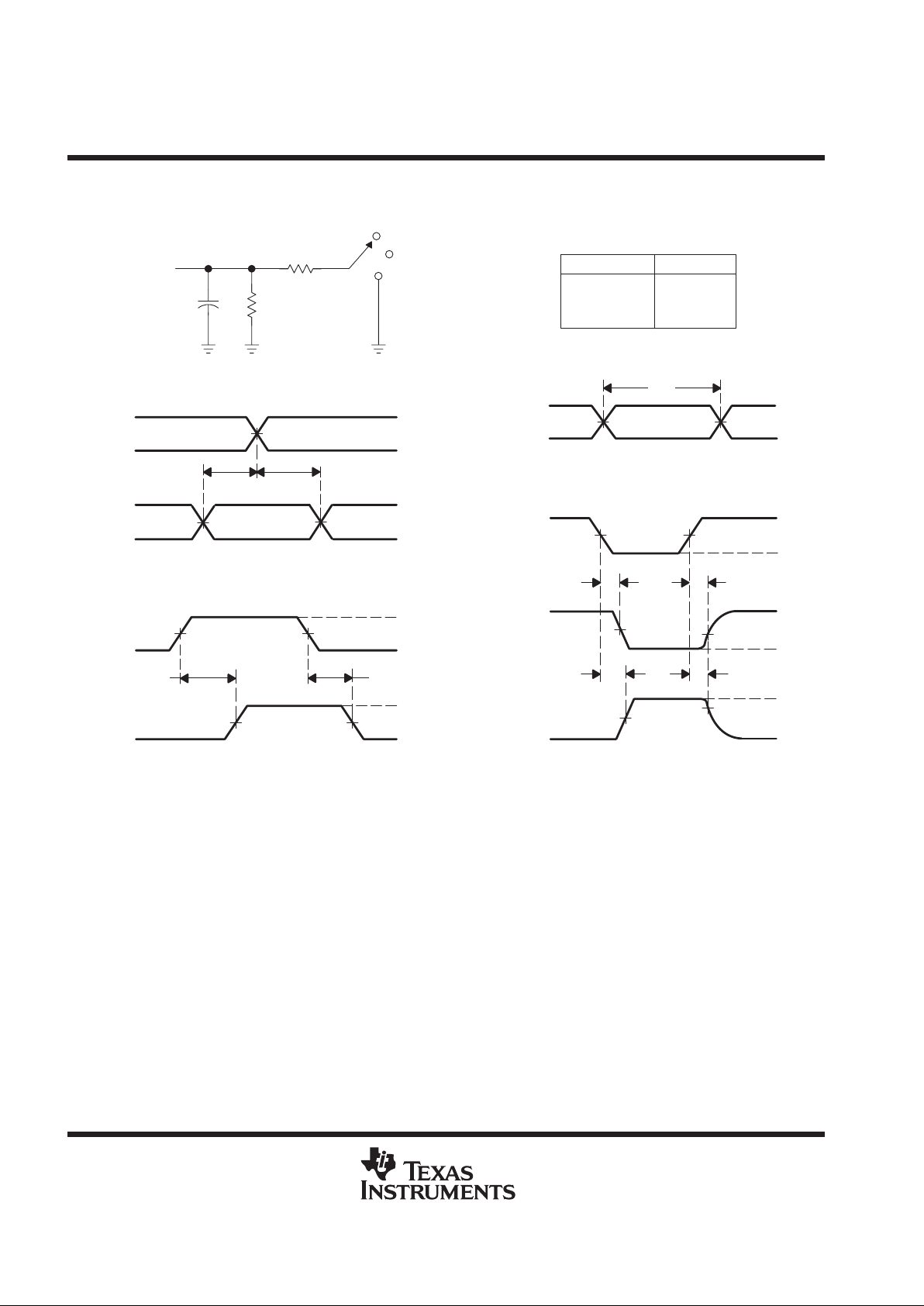
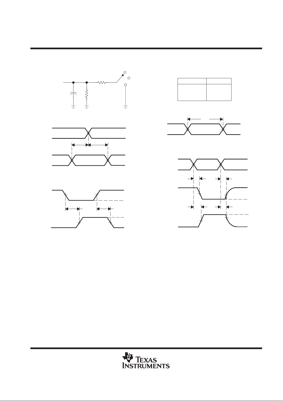
PARAMETER MEASUREMENT INFORMATION
V
CC
= 2.5 V ± 0.2 V
VCC/2
VCC/2
VCC/2VCC/2
VCC/2VCC/2
VCC/2
VCC/2
V
OH
V
OL
t
h
t
su
From Output
Under Test
CL = 30 pF
(see Note A)
LOAD CIRCUIT
S1
Open
GND
500 Ω
500 Ω
Output
Control
(low-level
enabling)
Output
Waveform 1
S1 at 2 × V
CC
(see Note B)
Output
Waveform 2
S1 at GND
(see Note B)
t
PZL
t
PZH
t
PLZ
t
PHZ
0 V
VOL + 0.15 V
VOH – 0.15 V
0 V
V
CC
0 V
0 V
t
w
V
CC
V
CC
VOLTAGE WAVEFORMS
SETUP AND HOLD TIMES
VOLTAGE WAVEFORMS
PULSE DURATION
VOLTAGE WAVEFORMS
ENABLE AND DISABLE TIMES
Timing
Input
Data
Input
Input
t
PLH/tPHL
t
PLZ/tPZL
t
PHZ/tPZH
Open
2 × V
CC
GND
TEST S1
NOTES: A. CL includes probe and jig capacitance.
B. Waveform 1 is for an output with internal conditions such that the output is low except when disabled by the output control.
Waveform 2 is for an output with internal conditions such that the output is high except when disabled by the output control.
C. All input pulses are supplied by generators having the following characteristics: PRR ≤ 10 MHz, ZO = 50 Ω, tr ≤ 2 ns, tf ≤ 2 ns.
D. The outputs are measured one at a time with one transition per measurement.
0 V
V
CC
VCC/2
t
PHL
VCC/2 VCC/2
V
CC
0 V
V
OH
V
OL
Input
Output
VOLTAGE WAVEFORMS
PROPAGATION DELAY TIMES
VCC/2 VCC/2
t
PLH
2 × V
CC
V
CC
Figure 1. Load Circuit and Voltage Waveforms
SN54ALVTH32373, SN74ALVTH32373
2.5-V/3.3-V 32-BIT TRANSPARENT D-TYPE LATCHES
WITH 3-STATE OUTPUTS
SCES322A – FEBRUARY 2000 – REVISED APRIL 2000
9
POST OFFICE BOX 655303 • DALLAS, TEXAS 75265
PARAMETER MEASUREMENT INFORMATION
V
CC
= 3.3 V ± 0.3 V
V
OH
V
OL
t
h
t
su
From Output
Under Test
CL = 50 pF
(see Note A)
LOAD CIRCUIT
S1
Open
GND
500 Ω
500 Ω
t
PLH
t
PHL
Output Control
Output
Waveform 1
S1 at 6 V
(see Note B)
Output
Waveform 2
S1 at GND
(see Note B)
t
PZL
t
PZH
t
PLZ
t
PHZ
3 V
0 V
V
OH
V
OL
0 V
VOL + 0.3 V
VOH – 0.3 V
≈ 0 V
3 V
0 V
0 V
t
w
Input
3 V
3 V
3 V
VOLTAGE WAVEFORMS
SETUP AND HOLD TIMES
VOLTAGE WAVEFORMS
PROPAGATION DELAY TIMES
INVERTING AND NONINVERTING OUTPUTS
VOLTAGE WAVEFORMS
PULSE DURATION
VOLTAGE WAVEFORMS
ENABLE AND DISABLE TIMES
LOW- AND HIGH-LEVEL ENABLING
Timing
Input
Data
Input
Output
Input
t
PLH/tPHL
t
PLZ/tPZL
t
PHZ/tPZH
Open
6 V
GND
TEST S1
NOTES: A. CL includes probe and jig capacitance.
B. Waveform 1 is for an output with internal conditions such that the output is low except when disabled by the output control.
Waveform 2 is for an output with internal conditions such that the output is high except when disabled by the output control.
C. All input pulses are supplied by generators having the following characteristics: PRR ≤ 10 MHz, ZO = 50 Ω, tr ≤ 2.5 ns, tf ≤ 2.5 ns.
D. The outputs are measured one at a time with one transition per measurement.
6 V
1.5 V
1.5 V 1.5 V
1.5 V 1.5 V
0 V
3 V
1.5 V
1.5 V
1.5 V 1.5 V
1.5 V
1.5 V
1.5 V 1.5 V
Figure 2. Load Circuit and Voltage Waveforms

IMPORTANT NOTICE
T exas Instruments and its subsidiaries (TI) reserve the right to make changes to their products or to discontinue
any product or service without notice, and advise customers to obtain the latest version of relevant information
to verify, before placing orders, that information being relied on is current and complete. All products are sold
subject to the terms and conditions of sale supplied at the time of order acknowledgment, including those
pertaining to warranty, patent infringement, and limitation of liability.
TI warrants performance of its semiconductor products to the specifications applicable at the time of sale in
accordance with TI’s standard warranty. Testing and other quality control techniques are utilized to the extent
TI deems necessary to support this warranty. Specific testing of all parameters of each device is not necessarily
performed, except those mandated by government requirements.
Customers are responsible for their applications using TI components.
In order to minimize risks associated with the customer’s applications, adequate design and operating
safeguards must be provided by the customer to minimize inherent or procedural hazards.
TI assumes no liability for applications assistance or customer product design. TI does not warrant or represent
that any license, either express or implied, is granted under any patent right, copyright, mask work right, or other
intellectual property right of TI covering or relating to any combination, machine, or process in which such
semiconductor products or services might be or are used. TI’s publication of information regarding any third
party’s products or services does not constitute TI’s approval, warranty or endorsement thereof.
Copyright 2000, Texas Instruments Incorporated
 Loading...