

Texas Instruments SN74ALVTH32244KR Datasheet
SN54ALVTH32244, SN74ALVTH32244
2.5-V/3.3-V 32-BIT BUFFERS/DRIVERS
WITH 3-STATE OUTPUTS
SCES279 – SEPTEMBER 1999
1
POST OFFICE BOX 655303 • DALLAS, TEXAS 75265
D
State-of-the-Art Advanced BiCMOS
Technology (ABT)
Widebus
Design for
2.5-V and 3.3-V Operation and Low Static
Power Dissipation
D
Support Mixed-Mode Signal Operation (5-V
Input and Output Voltages With 2.3-V to
3.6-V V
CC
)
D
T ypical V
OLP
(Output Ground Bounce)
<0.8 V at VCC = 3.3 V, TA = 25°C
D
High Drive (–24/24 mA at 2.5-V VCC and
–32/64 mA at 3.3-V VCC)
D
I
off
and Power-Up 3-State Support Hot
Insertion
D
Use Bus Hold on Data Inputs in Place of
External Pullup/Pulldown Resistors to
Prevent the Bus From Floating
NOTE: For tape and reel order entry:
The GKER package is abbreviated to KR.
D
Auto3-State Eliminates Bus Current
Loading When Output Exceeds VCC + 0.5 V
D
Flow-Through Architecture Facilitates
Printed Circuit Board Layout
D
Distributed VCC and GND Pin Configuration
Minimizes High-Speed Switching Noise
D
ESD Protection Exceeds JESD-22
– 2000-V Human-Body Model (A114-A)
– 200-V Machine Model (A115-A)
– 1000-V Charged-Device Model (C101)
D
Latch-Up Performance Exceeds 100 mA Per
JESD 78, Class II
D
Packaged in Plastic Fine-Pitch Ball Grid
Array Package
description
The ’ALVTH32244 devices are 32-bit buffers/line drivers designed for 2.5-V or 3.3-V VCC operation, but with
the capability to provide a TTL interface to a 5-V system environment. These devices can be used as eight 4-bit
buffers, four 8-bit buffers, two 16-bit buffers, or one 32-bit buffer. These devices provide true outputs and
symmetrical active-low output-enable (OE
) inputs.
When V
CC
is between 0 and 1.2-V , the devices are in the high-impedance state during power up or power down.
However, to ensure the high-impedance state above 1.2-V, OE
should be tied to VCC through a pullup resistor;
the minimum value of the resistor is determined by the current-sinking capability of the driver.
These devices are fully specified for hot-insertion applications using I
off
and power-up 3-state. The I
off
circuitry
disables the outputs, preventing damaging current backflow through the devices when they are powered down.
The power-up 3-state circuitry places the outputs in the high-impedance state during power up and power down,
which prevents driver conflict.
Active bus-hold circuitry is provided to hold unused or floating data inputs at a valid logic level.
The SN54ALVTH32244 is characterized for operation over the full military temperature range of –55°C to
125°C. The SN74ALVTH32244 is characterized for operation from –40°C to 85°C.
FUNCTION TABLE
(each 4-bit buffer)
INPUTS
OUTPUT
OE
A
Y
L H H
L LL
H X Z
Copyright 1999, Texas Instruments Incorporated
UNLESS OTHERWISE NOTED this document contains PRODUCTION
DATA information current as of publication date. Products conform to
specifications per the terms of Texas Instruments standard warranty.
Production processing does not necessarily include testing of all
parameters.
Please be aware that an important notice concerning availability, standard warranty, and use in critical applications of
Texas Instruments semiconductor products and disclaimers thereto appears at the end of this data sheet.
Widebus is a trademark of Texas Instruments Incorporated.
SN54ALVTH32244, SN74ALVTH32244
2.5-V/3.3-V 32-BIT BUFFERS/DRIVERS
WITH 3-STATE OUTPUTS
SCES279 – SEPTEMBER 1999
2
POST OFFICE BOX 655303 • DALLAS, TEXAS 75265
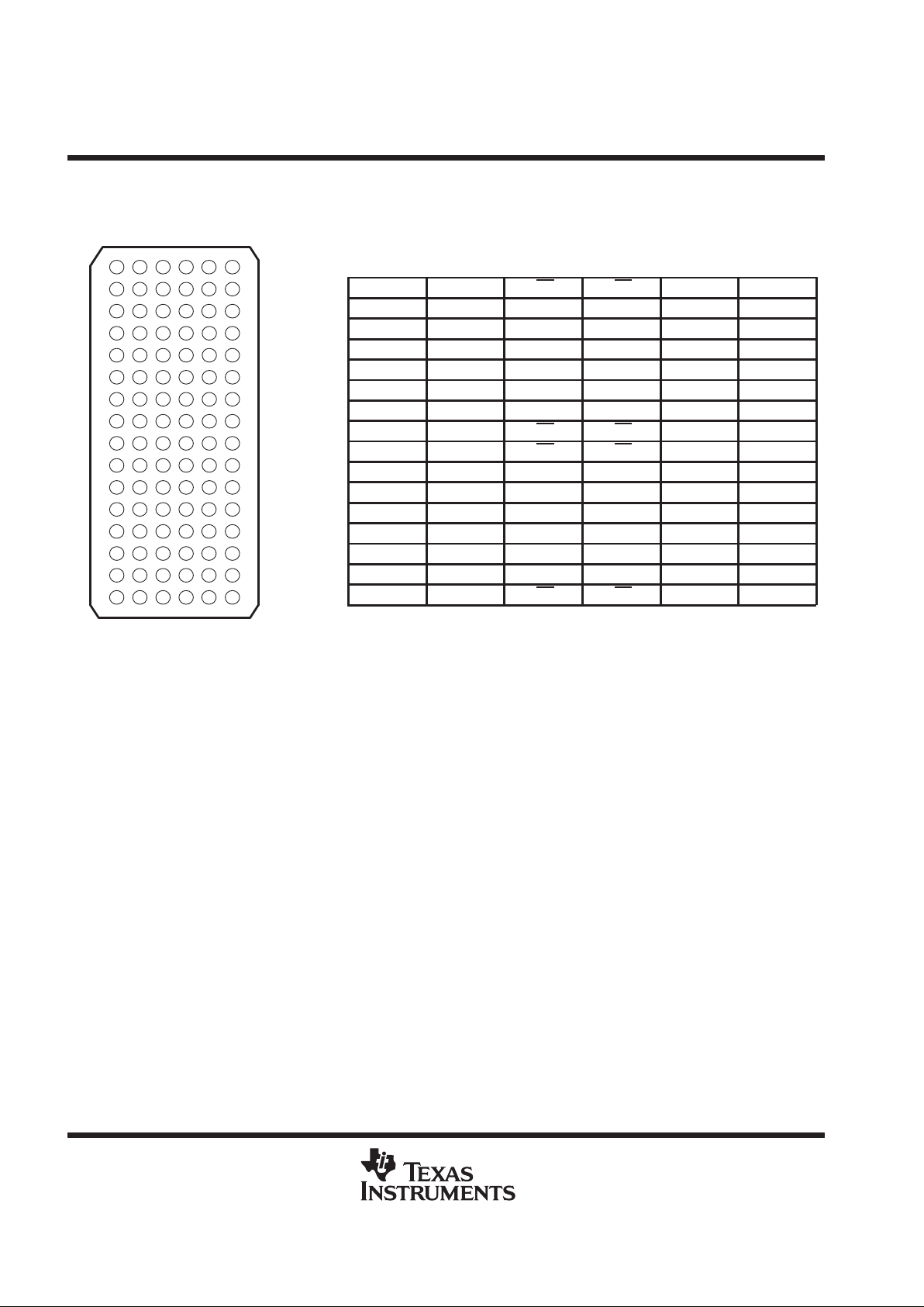
terminal assignments
123456
A 1Y2
1Y1 1OE 2OE 1A1 1A2
B 1Y4 1Y3 GND GND 1A3 1A4
C 2Y2 2Y1 1V
CC
1V
CC
2A1 2A2
D 2Y4 2Y3 GND GND 2A3 2A4
E 3Y2 3Y1 GND GND 3A1 3A2
F 3Y4 3Y3 1V
CC
1V
CC
3A3 3A4
G 4Y2 4Y1 GND GND 4A1 4A2
H 4Y3 4Y4 4OE 3OE 4A4 4A3
J 5Y2 5Y1 5OE 6OE 5A1 5A2
K 5Y4 5Y3 GND GND 5A3 5A4
L 6Y2 6Y1 2V
CC
2V
CC
6A1 6A2
M 6Y4 6Y3 GND GND 6A3 6A4
N 7Y2 7Y1 GND GND 7A1 7A2
P 7Y4 7Y3 2V
CC
2V
CC
7A3 7A4
R 8Y2 8Y1 GND GND 8A1 8A2
T 8Y3 8Y4 8OE 7OE 8A4 8A3
GKE PACKAGE
(TOP VIEW)
J
H
G
F
E
D
C
B
A
213465
P
N
M
L
K
T
R
SN54ALVTH32244, SN74ALVTH32244
2.5-V/3.3-V 32-BIT BUFFERS/DRIVERS
WITH 3-STATE OUTPUTS
SCES279 – SEPTEMBER 1999
3
POST OFFICE BOX 655303 • DALLAS, TEXAS 75265
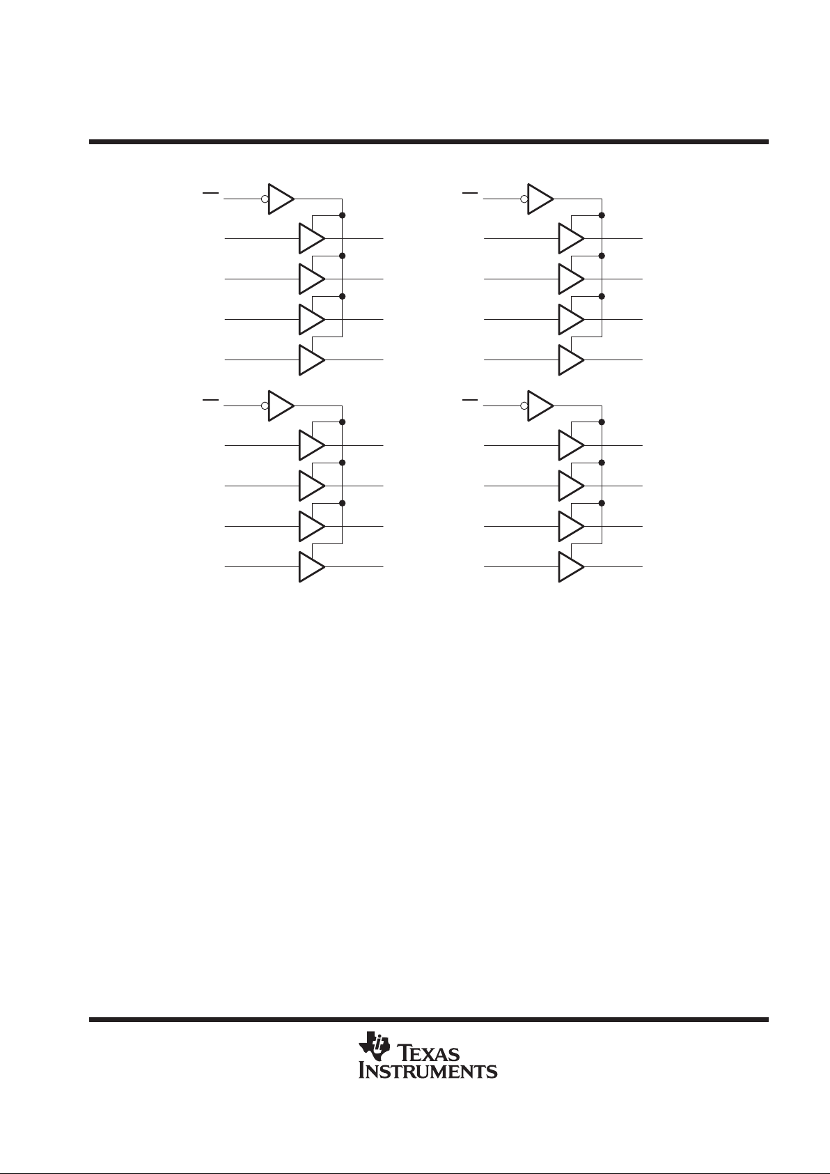
logic diagram (positive logic)
1OE
1A1
1A2
1A3
1A4
1Y1
1Y2
1Y3
1Y4
A3
A5
A6
B5
B6
A2
A1
B2
B1
2OE
2A1
2A2
2A3
2A4
2Y1
2Y2
2Y3
2Y4
A4
C5
C6
D5
D6
C2
C1
D2
D1
3OE
3A1
3A2
3A3
3A4
3Y1
3Y2
3Y3
3Y4
H4
E5
E6
F5
F6
E2
E1
F2
F1
4OE
4A1
4A2
4A3
4A4
4Y1
4Y2
4Y3
4Y4
H3
G5
G6
H6
H5
G2
G1
H1
H2
NOTE A: 1VCC is associated with these channels.
SN54ALVTH32244, SN74ALVTH32244
2.5-V/3.3-V 32-BIT BUFFERS/DRIVERS
WITH 3-STATE OUTPUTS
SCES279 – SEPTEMBER 1999
4
POST OFFICE BOX 655303 • DALLAS, TEXAS 75265
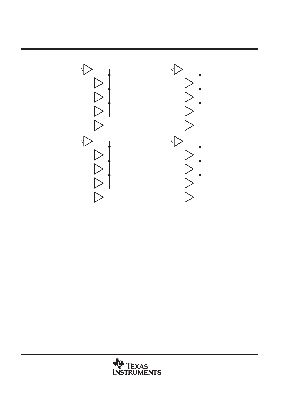
logic diagram (positive logic)
5OE
5A1
5A2
5A3
5A4
5Y1
5Y2
5Y3
5Y4
J3
J5
J6
K5
K6
J2
J1
K2
K1
6OE
6A1
6A2
6A3
6A4
6Y1
6Y2
6Y3
6Y4
J4
L5
L6
M5
M6
L2
L1
M2
M1
7OE
7A1
7A2
7A3
7A4
7Y1
7Y2
7Y3
7Y4
T4
N5
N6
P5
P6
N2
N1
P2
P1
8OE
8A1
8A2
8A3
8A4
8Y1
8Y2
8Y3
8Y4
T3
R5
R6
T6
T5
R2
R1
T1
T2
NOTE A: 2VCC is associated with these channels.
absolute maximum ratings over operating free-air temperature range (unless otherwise noted)
†
Supply voltage range, VCC –0.5 V to 4.6 V. . . . . . . . . . . . . . . . . . . . . . . . . . . . . . . . . . . . . . . . . . . . . . . . . . . . . . . . .
Input voltage range, VI (see Note 1) –0.5 V to 7 V. . . . . . . . . . . . . . . . . . . . . . . . . . . . . . . . . . . . . . . . . . . . . . . . . .
Voltage range applied to any output in the high-impedance
or power-off state, V
O
(see Note 1) –0.5 V to 7 V. . . . . . . . . . . . . . . . . . . . . . . . . . . . . . . . . . . . . . . . . . . . . . . .
Voltage range applied to any output in the high state, VO (see Note 1) –0.5 V to 7 V. . . . . . . . . . . . . . . . . . . .
Current into any output in the low state, IO: SN54ALVTH32244 96 mA. . . . . . . . . . . . . . . . . . . . . . . . . . . . . . . .
SN74ALVTH32244 128 mA. . . . . . . . . . . . . . . . . . . . . . . . . . . . . . .
Current into any output in the high state, I
O
(see Note 2): SN54ALVTH32244 48 mA. . . . . . . . . . . . . . . . . . . .
SN74ALVTH32244 64 mA. . . . . . . . . . . . . . . . . . . .
Input clamp current, I
IK
(V
I
< 0) –50 mA. . . . . . . . . . . . . . . . . . . . . . . . . . . . . . . . . . . . . . . . . . . . . . . . . . . . . . . . . . .
Output clamp current, I
OK
(V
O
< 0) –50 mA. . . . . . . . . . . . . . . . . . . . . . . . . . . . . . . . . . . . . . . . . . . . . . . . . . . . . . . .
Package thermal impedance, θ
JA
(see Note 3) 40°C/W. . . . . . . . . . . . . . . . . . . . . . . . . . . . . . . . . . . . . . . . . . . . .
Storage temperature range, T
stg
–65°C to 150°C. . . . . . . . . . . . . . . . . . . . . . . . . . . . . . . . . . . . . . . . . . . . . . . . . . .
†
Stresses beyond those listed under “absolute maximum ratings” may cause permanent damage to the device. These are stress ratings only, and
functional operation of the device at these or any other conditions beyond those indicated under “recommended operating conditions” is not
implied. Exposure to absolute-maximum-rated conditions for extended periods may affect device reliability.
NOTES: 1. The input and output negative-voltage ratings may be exceeded if the input and output clamp-current ratings are observed.
2. This current flows only when the output is in the high state and VO > VCC.
3. The package thermal impedance is calculated in accordance with JESD 51.
 Loading...