

Texas Instruments SN74ALVTH16601DL, SN74ALVTH16601DLR, SN74ALVTH16601GR, SN74ALVTH16601VR Datasheet
SN54ALVTH16601, SN74ALVTH16601
2.5-V/3.3-V 18-BIT UNIVERSAL BUS TRANSCEIVER
WITH 3-STATE OUTPUTS
SCES143A – SEPTEMBER 1998 – REVISED JUL Y 1999
1
POST OFFICE BOX 655303 • DALLAS, TEXAS 75265
D
UBT
(Universal Bus Transceiver)
Combines D-Type Latches and D-Type
Flip-Flops for Operation in Transparent,
Latched, Clocked, or Clock-Enabled Mode
D
State-of-the-Art Advanced BiCMOS
Technology (ABT)
Widebus
Design for
2.5-V and 3.3-V Operation and Low
Static-Power Dissipation
D
Support Mixed-Mode Signal Operation (5-V
Input and Output Voltages With 2.3-V to
3.6-V V
CC
)
D
T ypical V
OLP
(Output Ground Bounce)
<0.8 V at V
CC
= 3.3 V, TA = 25°C
D
High-Drive (–24/24 mA at 2.5-V and
–32/64 mA at 3.3-V V
CC
)
D
I
off
and Power-Up 3-State Support Hot
Insertion
D
Use Bus Hold on Data Inputs in Place of
External Pullup/Pulldown Resistors to
Prevent the Bus From Floating
D
Auto3-State Eliminates Bus Current
Loading When Output Exceeds V
CC
+ 0.5 V
D
Flow-Through Architecture Facilitates
Printed Circuit Board Layout
D
Distributed VCC and GND Pin Configuration
Minimizes High-Speed Switching Noise
D
ESD Protection Exceeds 2000 V Per
MIL-STD-883, Method 3015; Exceeds 200 V
Using Machine Model (C = 200 pF, R = 0)
D
Latch-Up Performance Exceeds 100 mA Per
JESD 78, Class II
D
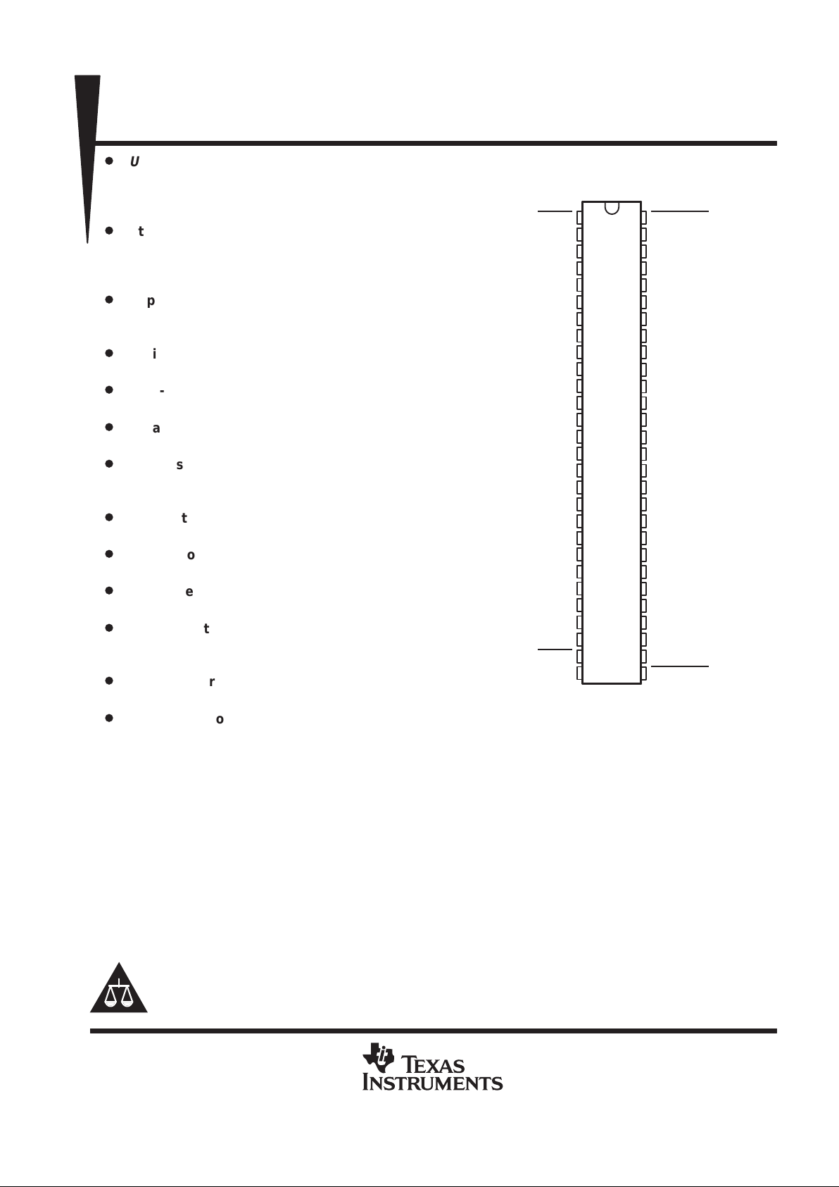
Package Options Include Plastic Shrink
Small-Outline (DL), Thin Shrink
Small-Outline (DGG), Thin Very
Small-Outline (DGV) Packages, and 380-mil
Fine-Pitch Ceramic Flat (WD) Package
NOTE: For tape and reel order entry:
The DGGR package is abbreviated to GR and
the DGVR package is abbreviated to VR.
description
The ’AL VTH16601 devices are 18-bit universal bus transceivers designed for 2.5-V or 3.3-V VCC operation, but
with the capability to provide a TTL interface to a 5-V system environment.
The devices combine D-type latches and D-type flip-flops to allow data flow in transparent, latched, and clocked
modes.
Copyright 1999, Texas Instruments Incorporated
Please be aware that an important notice concerning availability, standard warranty, and use in critical applications of
Texas Instruments semiconductor products and disclaimers thereto appears at the end of this data sheet.
UBT and Widebus are trademarks of Texas Instruments Incorporated.
1
2
3
4
5
6
7
8
9
10
11
12
13
14
15
16
17
18
19
20
21
22
23
24
25
26
27
28
56
55
54
53
52
51
50
49
48
47
46
45
44
43
42
41
40
39
38
37
36
35
34
33
32
31
30
29
OEAB
LEAB
A1
GND
A2
A3
V
CC
A4
A5
A6
GND
A7
A8
A9
A10
A1 1
A12
GND
A13
A14
A15
V
CC
A16
A17
GND
A18
OEBA
LEBA
CLKENAB
CLKAB
B1
GND
B2
B3
V
CC
B4
B5
B6
GND
B7
B8
B9
B10
B1 1
B12
GND
B13
B14
B15
V
CC
B16
B17
GND
B18
CLKBA
CLKENBA
SN54ALVTH16601. . . WD PACKAGE
SN74ALVTH16601. . . DGG, DGV, OR DL PACKAGE
(TOP VIEW)
UNLESS OTHERWISE NOTED this document contains PRODUCTION
DATA information current as of publication date. Products conform to
specifications per the terms of Texas Instruments standard warranty.
Production processing does not necessarily include testing of all
parameters.
SN54ALVTH16601, SN74ALVTH16601
2.5-V/3.3-V 18-BIT UNIVERSAL BUS TRANSCEIVER
WITH 3-STATE OUTPUTS
SCES143A – SEPTEMBER 1998 – REVISED JUL Y 1999
2
POST OFFICE BOX 655303 • DALLAS, TEXAS 75265
description (continued)
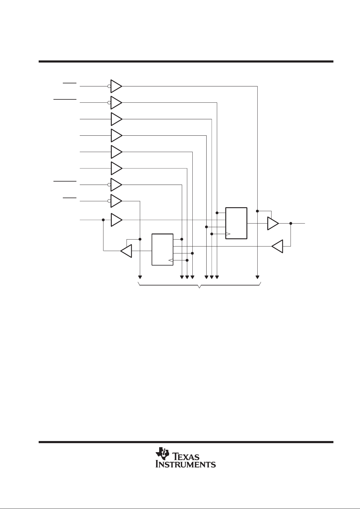
Data flow in each direction is controlled by output-enable (OEAB and OEBA), latch-enable (LEAB and LEBA),
and clock (CLKAB and CLKBA) inputs. The clock can be controlled by the clock-enable (CLKENAB
and
CLKENBA
) inputs. For A-to-B data flow, the device operates in the transparent mode when LEAB is high. When
LEAB is low, the A data is latched if CLKAB is held at a high or low logic level. If LEAB is low , the A data is stored
in the latch/flip-flop on the low-to-high transition of CLKAB. Output enable OEAB
is active low. When OEAB is
low, the outputs are active. When OEAB
is high, the outputs are in the high-impedance state.
Data flow for B to A is similar to that of A to B, but uses OEBA
, LEBA, CLKBA, and CLKENBA.
This device is fully specified for hot-insertion applications using I
off
and power-up 3-state. The I
off
circuitry
disables the outputs, preventing damaging current backflow through the device when it is powered down. The
power-up 3-state circuitry places the outputs in the high-impedance state during power up and power down,
which prevents driver conflict.
When V
CC
is between 0 and 1.2 V , the device is in the high-impedance state during power up or power down.
However, to ensure the high-impedance state above 1.2 V, OE
should be tied to VCC through a pullup resistor;
the minimum value of the resistor is determined by the current-sinking capability of the driver.
Active bus-hold circuitry is provided to hold unused or floating data inputs at a valid logic level.
The SN54ALVTH16601 is characterized for operation over the full military temperature range of –55°C to
125°C. The SN74ALVTH16601 is characterized for operation from –40°C to 85°C.
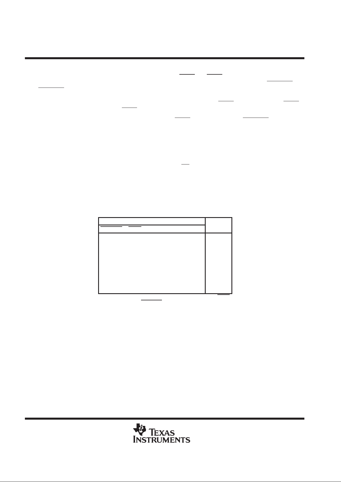
FUNCTION TABLE
†
INPUTS
OUTPUT
CLKENAB OEAB LEAB
CLKAB A
B
X H X X X Z
X LH XL L
X LH XH H
H LL XXB
0
‡
H LL XXB
0
‡
L LL ↑LL
L LL ↑HH
L LLL or H X B
0
‡
†
A-to-B data flow is shown: B-to-A flow is similar but uses OEBA,
LEBA, CLKBA, and CLKENBA
.
‡
Output level before the indicated steady-state input conditions were
established
SN54ALVTH16601, SN74ALVTH16601
2.5-V/3.3-V 18-BIT UNIVERSAL BUS TRANSCEIVER
WITH 3-STATE OUTPUTS
SCES143A – SEPTEMBER 1998 – REVISED JUL Y 1999
3
POST OFFICE BOX 655303 • DALLAS, TEXAS 75265
logic diagram (positive logic)
CE
1D
C1
CLK
CE
1D
C1
CLK
B1
OEAB
CLKENAB
CLKAB
LEAB
LEBA
CLKBA
CLKENBA
OEBA
A1
1
56
55
2
28
30
29
27
3
54
To 17 Other Channels
SN54ALVTH16601, SN74ALVTH16601
2.5-V/3.3-V 18-BIT UNIVERSAL BUS TRANSCEIVER
WITH 3-STATE OUTPUTS
SCES143A – SEPTEMBER 1998 – REVISED JUL Y 1999
4
POST OFFICE BOX 655303 • DALLAS, TEXAS 75265
absolute maximum ratings over operating free-air temperature range (unless otherwise noted)
†
Supply voltage range, V
CC
–0.5 V to 4.6 V. . . . . . . . . . . . . . . . . . . . . . . . . . . . . . . . . . . . . . . . . . . . . . . . . . . . . . . . .
Input voltage range, V
I
(see Note 1) –0.5 V to 7 V. . . . . . . . . . . . . . . . . . . . . . . . . . . . . . . . . . . . . . . . . . . . . . . . . .
Voltage range applied to any output in the high or power-off state, V
O
(see Note 1) –0.5 V to 7 V. . . . . . . . .
Output current in the low state, I
O
: SN54ALVTH16601 96 mA. . . . . . . . . . . . . . . . . . . . . . . . . . . . . . . . . . . . . . . .
SN74ALVTH16601 128 mA. . . . . . . . . . . . . . . . . . . . . . . . . . . . . . . . . . . . . . .
Output current in the high state, I
O
: SN54ALVTH16601 –48 mA. . . . . . . . . . . . . . . . . . . . . . . . . . . . . . . . . . . . . .
SN74ALVTH16601 –64 mA. . . . . . . . . . . . . . . . . . . . . . . . . . . . . . . . . . . . . .
Input clamp current, I
IK
(V
I
< 0) –50 mA. . . . . . . . . . . . . . . . . . . . . . . . . . . . . . . . . . . . . . . . . . . . . . . . . . . . . . . . . . .
Output clamp current, I
OK
(V
O
< 0) –50 mA. . . . . . . . . . . . . . . . . . . . . . . . . . . . . . . . . . . . . . . . . . . . . . . . . . . . . . . .
Package thermal impedance, θ
JA
(see Note 2): DGG package 81°C/W. . . . . . . . . . . . . . . . . . . . . . . . . . . . . . .
DGV package 86°C/W. . . . . . . . . . . . . . . . . . . . . . . . . . . . . . . .
DL package 74°C/W. . . . . . . . . . . . . . . . . . . . . . . . . . . . . . . . .
Storage temperature range, T
stg
–65°C to 150°C. . . . . . . . . . . . . . . . . . . . . . . . . . . . . . . . . . . . . . . . . . . . . . . . . . .
†
Stresses beyond those listed under “absolute maximum ratings” may cause permanent damage to the device. These are stress ratings only, and
functional operation of the device at these or any other conditions beyond those indicated under “recommended operating conditions” is not
implied. Exposure to absolute-maximum-rated conditions for extended periods may affect device reliability.
NOTES: 1. The input and output negative-voltage ratings may be exceeded if the input and output clamp-current ratings are observed.
2. The package thermal impedance is calculated in accordance with JESD 51.
recommended operating conditions, VCC = 2.5 V ± 0.2 V (see Note 3)
SN54ALVTH16601 SN74ALVTH16601
MIN TYP MAX MIN TYP MAX
UNIT
V
CC
Supply voltage 2.3 2.7 2.3 2.7 V
V
IH
High-level input voltage 1.7 1.7 V
V
IL
Low-level input voltage 0.7 0.7 V
V
I
Input voltage 0 V
CC
5.5 0 V
CC
5.5 V
I
OH
High-level output current –6 –8 mA
Low-level output current 6 8
I
OL
Low-level output current; current duty cycle ≤ 50%; f ≥ 1 kHz 18 24
mA
∆t/∆v Input transition rise or fall rate Outputs enabled 10 10 ns/V
∆t/∆V
CC
Power-up ramp rate 200 200 µs/V
T
A
Operating free-air temperature –55 125 –40 85 °C
NOTE 3: All unused control inputs of the device must be held at VCC or GND to ensure proper device operation. Refer to the TI application report,
Implications of Slow or Floating CMOS Inputs
, literature number SCBA004.
PRODUCT PREVIEW information concerns products in the formative or
design phase of development. Characteristic data and other
specifications are design goals. Texas Instruments reserves the right to
change or discontinue these products without notice.
 Loading...