

Texas Instruments SN74ALVCH32501GKFR, SN74ALVCH32501KR Datasheet
SN74ALVCH32501
36-BIT UNIVERSAL BUS TRANSCEIVER
WITH 3-STATE OUTPUTS
SCES144C – OCTOBER 1998 – REVISED MAY 2000
1
POST OFFICE BOX 655303 • DALLAS, TEXAS 75265
D
Member of the Texas Instruments
Widebus
Family
D
EPIC
(Enhanced-Performance Implanted
CMOS) Submicron Process
D
UBT
(Universal Bus Transceiver)
Combines D-Type Latches and D-Type
Flip-Flops for Operation in Transparent,
Latched, or Clocked Mode
D
Bus Hold on Data Inputs Eliminates the
Need for External Pullup/Pulldown
Resistors
D
ESD Protection Exceeds 2000 V Per
MIL-STD-883, Method 3015; Exceeds 200 V
Using Machine Model (C = 200 pF, R = 0)
D
Latch-Up Performance Exceeds 250 mA Per
JESD 17
D
Packaged in Plastic Fine-Pitch Ball Grid
Array Package
description
This 36-bit universal bus transceiver is designed for 1.65-V to 3.6-V VCC operation.
This device can be used as two 18-bit transceivers or one 36-bit transceiver. Data flow in each direction is
controlled by output-enable (OEAB and OEBA), latch-enable (LEAB and LEBA), and clock (CLKAB and
CLKBA) inputs. For A-to-B data flow, the device operates in the transparent mode when LEAB is high. When
LEAB is low, the A data is latched if CLKAB is held at a high or low logic level. If LEAB is low , the A data is stored
in the latch/flip-flop on the low-to-high transition of CLKAB. When OEAB is high, the outputs are active. When
OEAB is low , the outputs are in the high-impedance state.
Data flow for B to A is similar to that of A to B, but uses OEBA, LEBA, and CLKBA. The output enables are
complementary (OEAB is active high and OEBA is active low).
To ensure the high-impedance state during power up or power down, OEBA should be tied to VCC through a
pullup resistor and OEAB should be tied to GND through a pulldown resistor; the minimum value of the resistor
is determined by the current-sinking capability of the driver.
Active bus-hold circuitry is provided to hold unused or floating data inputs at a valid logic level.
The SN74ALVCH32501 is characterized for operation from –40°C to 85°C.
FUNCTION TABLE
†
INPUTS
OUTPUT
OEAB LEAB CLKAB A
B
L X X X Z
H HXLL
H HXHH
H L ↑ LL
H L ↑ HH
H LHXB
0
‡
H L L X
B
0
§
†
A-to-B data flow is shown; B-to-A flow is similar but
uses OEBA
, LEBA, and CLKBA.
‡
Output level before the indicated steady-state input
conditions were established, provided that CLKAB
was high before LEAB went low
§
Output level before the indicated steady-state input
conditions were established
Copyright 2000, Texas Instruments Incorporated
Please be aware that an important notice concerning availability, standard warranty, and use in critical applications of
Texas Instruments semiconductor products and disclaimers thereto appears at the end of this data sheet.
EPIC, UBT, and Widebus are trademarks of Texas Instruments.
PRODUCTION DATA information is current as of publication date.
Products conform to specifications per the terms of Texas Instruments
standard warranty. Production processing does not necessarily include
testing of all parameters.
SN74ALVCH32501
36-BIT UNIVERSAL BUS TRANSCEIVER
WITH 3-STATE OUTPUTS
SCES144C – OCTOBER 1998 – REVISED MAY 2000
2
POST OFFICE BOX 655303 • DALLAS, TEXAS 75265
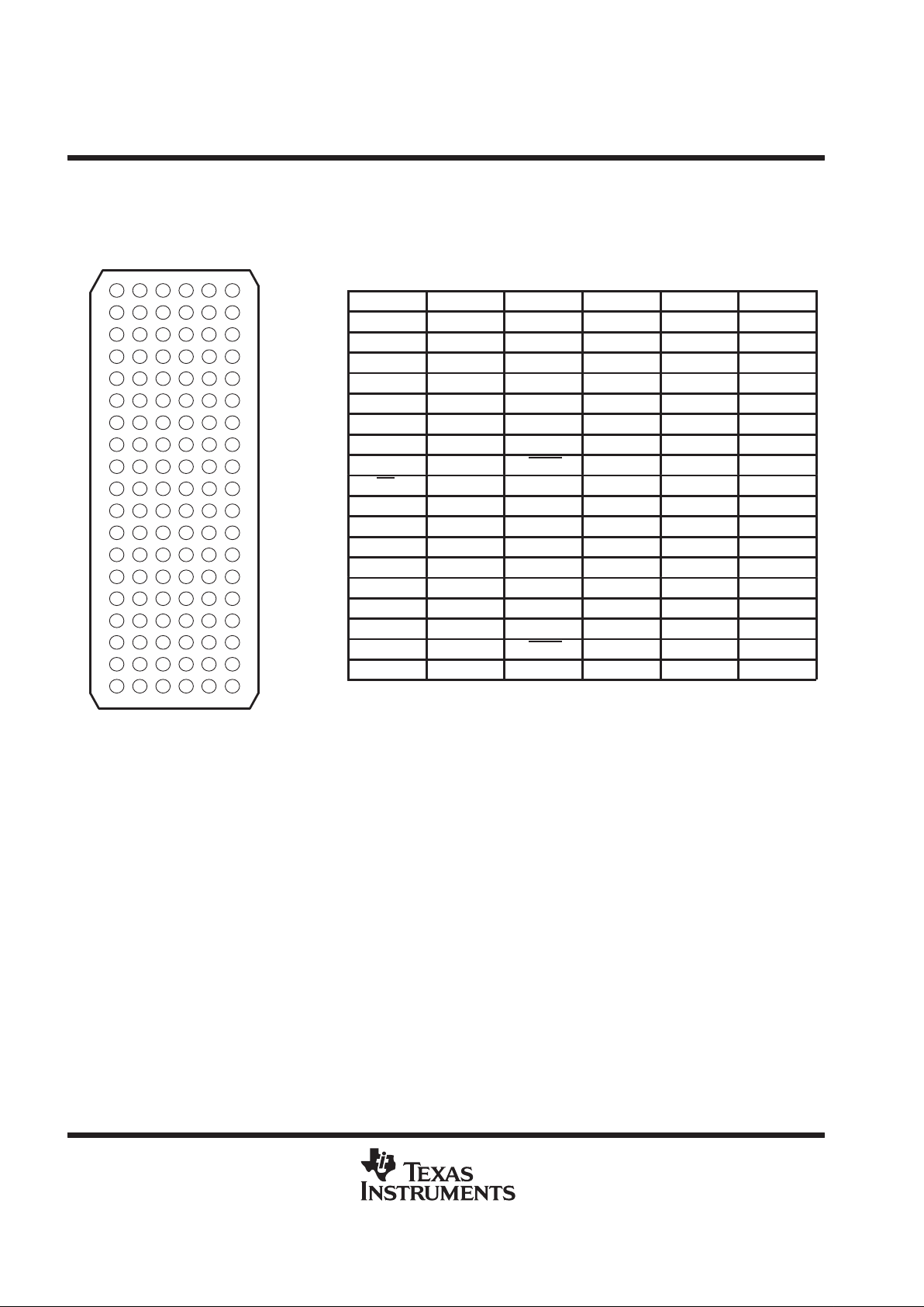
terminal assignments
123456
A 1A2
1A1 1LEAB 1CLKAB 1B1 1B2
B 1A4 1A3 1OEAB GND 1B3 1B4
C 1A6 1A5 GND GND 1B5 1B6
D 1A8 1A7 V
CC
V
CC
1B7 1B8
E 1A10 1A9 GND GND 1B9 1B10
F 1A12 1A11 GND GND 1B11 1B12
G 1A14 1A13 V
CC
V
CC
1B13 1B14
H 1A15 1A16 GND GND 1B16 1B15
J 1A17 1A18 1OEBA 1CLKBA 1B18 1B17
K NC 2LEAB 1LEBA GND 2CLKAB NC
L 2A2 2A1 2OEAB GND 2B1 2B2
M 2A4 2A3 GND GND 2B3 2B4
N 2A6 2A5 V
CC
V
CC
2B5 2B6
P 2A8 2A7 GND GND 2B7 2B8
R 2A10 2A9 GND GND 2B9 2B10
T 2A12 2A11 V
CC
V
CC
2B11 2B12
U 2A14 2A13 GND GND 2B13 2B14
V 2A15 2A16 2OEBA 2CLKBA 2B16 2B15
W 2A17 2A18 2LEBA GND 2B18 2B17
GKF PACKAGE
(TOP VIEW)
J
H
G
F
E
D
C
B
A
213465
P
N
M
L
K
T
R
U
W
V
NC – No internal connection
SN74ALVCH32501
36-BIT UNIVERSAL BUS TRANSCEIVER
WITH 3-STATE OUTPUTS
SCES144C – OCTOBER 1998 – REVISED MAY 2000
3
POST OFFICE BOX 655303 • DALLAS, TEXAS 75265
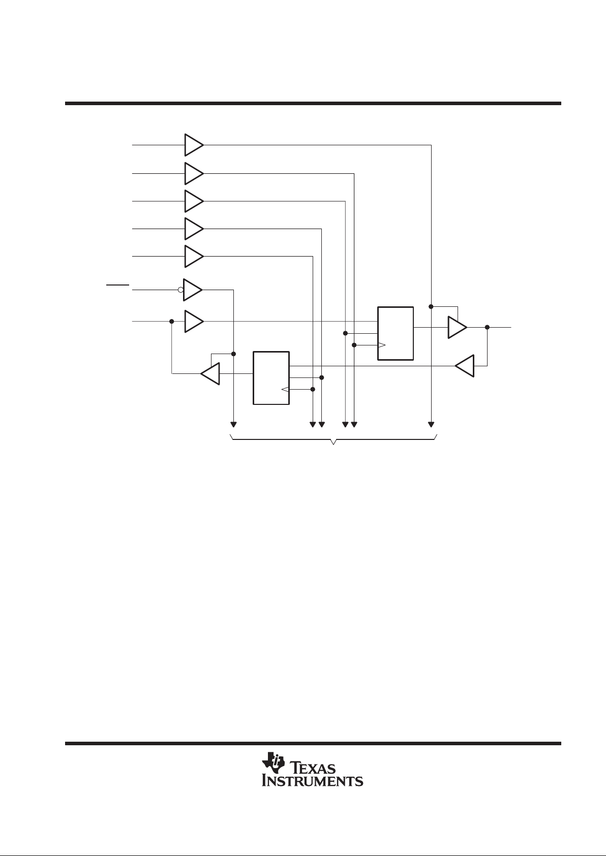
logic diagram (positive logic)
1D
C1
CLK
1D
C1
CLK
1B1
1OEAB
1CLKAB
1LEAB
1LEBA
1CLKBA
1OEBA
1A1
B3
A4
A3
K3
J4
J3
A2
A5
To 17 Other Channels
SN74ALVCH32501
36-BIT UNIVERSAL BUS TRANSCEIVER
WITH 3-STATE OUTPUTS
SCES144C – OCTOBER 1998 – REVISED MAY 2000
4
POST OFFICE BOX 655303 • DALLAS, TEXAS 75265
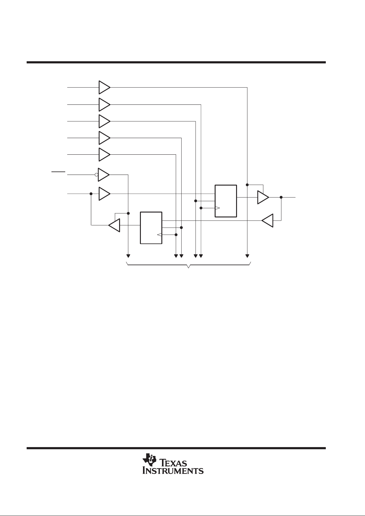
logic diagram (positive logic)
1D
C1
CLK
1D
C1
CLK
2B1
2OEAB
2CLKAB
2LEAB
2LEBA
2CLKBA
2OEBA
2A1
L3
K5
K2
W3
V4
V3
L2
L5
To 17 Other Channels
absolute maximum ratings over operating free-air temperature range (unless otherwise noted)
†
Supply voltage range, V
CC
–0.5 V to 4.6 V. . . . . . . . . . . . . . . . . . . . . . . . . . . . . . . . . . . . . . . . . . . . . . . . . . . . . . . . .
Input voltage range, V
I
: Except I/O ports (see Note 1) –0.5 V to 4.6 V. . . . . . . . . . . . . . . . . . . . . . . . . . . . . . . . .
I/O ports (see Notes 1 and 2) –0.5 V to VCC + 0.5 V. . . . . . . . . . . . . . . . . . . . . . . . . . .
Output voltage range, VO (see Notes 1 and 2) –0.5 V to VCC + 0.5 V. . . . . . . . . . . . . . . . . . . . . . . . . . . . . . . . . .
Input clamp current, IIK (VI < 0) –50 mA. . . . . . . . . . . . . . . . . . . . . . . . . . . . . . . . . . . . . . . . . . . . . . . . . . . . . . . . . . .
Output clamp current, IOK (VO < 0) –50 mA. . . . . . . . . . . . . . . . . . . . . . . . . . . . . . . . . . . . . . . . . . . . . . . . . . . . . . . .
Continuous output current, I
O
±50 mA. . . . . . . . . . . . . . . . . . . . . . . . . . . . . . . . . . . . . . . . . . . . . . . . . . . . . . . . . . . . .
Continuous current through each VCC or GND ±100 mA. . . . . . . . . . . . . . . . . . . . . . . . . . . . . . . . . . . . . . . . . . . . .
Package thermal impedance, θ
JA
(see Note 3) 39°C/W. . . . . . . . . . . . . . . . . . . . . . . . . . . . . . . . . . . . . . . . . . . . .
Storage temperature range, T
stg
–65°C to 150°C. . . . . . . . . . . . . . . . . . . . . . . . . . . . . . . . . . . . . . . . . . . . . . . . . . .
†
Stresses beyond those listed under “absolute maximum ratings” may cause permanent damage to the device. These are stress ratings only, and
functional operation of the device at these or any other conditions beyond those indicated under “recommended operating conditions” is not
implied. Exposure to absolute-maximum-rated conditions for extended periods may affect device reliability.
NOTES: 1. The input negative-voltage and output voltage ratings may be exceeded if the input and output-current ratings are observed.
2. This value is limited to 4.6 V maximum.
3. The package thermal impedance is calculated in accordance with JESD 51.
 Loading...