

Texas Instruments SN74ALVCH245DGVR, SN74ALVCH245DW, SN74ALVCH245DWR, SN74ALVCH245PWR Datasheet
OPERATION
SN74ALVCH245
OCTAL BUS TRANSCEIVER
WITH 3-STATE OUTPUTS
SCES119D – JULY 1997 – REVISED MAY 1999
D
EPIC
(Enhanced-Performance Implanted
CMOS) Submicron Process
D
Latch-Up Performance Exceeds 100 mA Per
JESD 78, Class II
D
Bus Hold on Data Inputs Eliminates the
Need for External Pullup/Pulldown
Resistors
D
Package Options Include Plastic
Small-Outline (DW), Thin Very
Small-Outline (DGV), and Thin Shrink
Small-Outline (PW) Packages
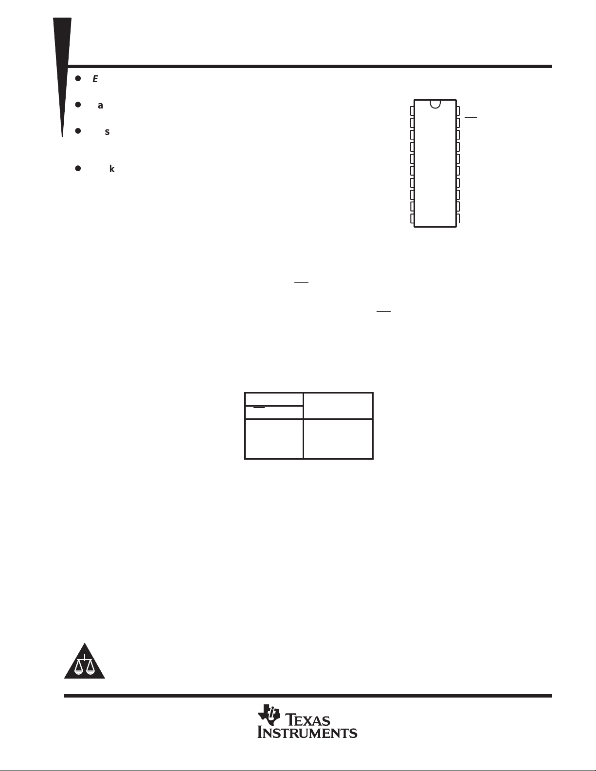
DGV, DW, OR PW PACKAGE
DIR
A1
A2
A3
A4
A5
A6
A7
A8
GND
(TOP VIEW)
1
20
2
19
3
18
4
17
5
16
6
15
7
14
8
13
9
12
10
11
V
OE
B1
B2
B3
B4
B5
B6
B7
B8
CC
description
This octal bus transceiver is designed for 1.65-V to 3.6-V VCC operation.
The SN74AL VCH245 is designed for asynchronous communication between data buses. The device transmits
data from the A bus to the B bus or from the B bus to the A bus, depending on the logic level at the
direction-control (DIR) input. The output-enable (OE
effectively isolated.
T o ensure the high-impedance state during power up or power down, OE
resistor; the minimum value of the resistor is determined by the current-sinking capability of the driver.
Active bus-hold circuitry is provided to hold unused or floating data inputs at a valid logic level.
) input can be used to disable the device so the buses are
should be tied to VCC through a pullup
The SN74ALVCH245 is characterized for operation from –40°C to 85°C.
FUNCTION TABLE
INPUTS
OE DIR
L L B data to A bus
L H A data to B bus
H X Isolation
Please be aware that an important notice concerning availability, standard warranty, and use in critical applications of
Texas Instruments semiconductor products and disclaimers thereto appears at the end of this data sheet.
EPIC is a trademark of Texas Instruments Incorporated.
PRODUCTION DATA information is current as of publication date.
Products conform to specifications per the terms of Texas Instruments
standard warranty. Production processing does not necessarily include
testing of all parameters.
POST OFFICE BOX 655303 • DALLAS, TEXAS 75265
Copyright 1999, Texas Instruments Incorporated
1
SN74ALVCH245
OCTAL BUS TRANSCEIVER
WITH 3-STATE OUTPUTS
SCES119D – JULY 1997 – REVISED MAY 1999
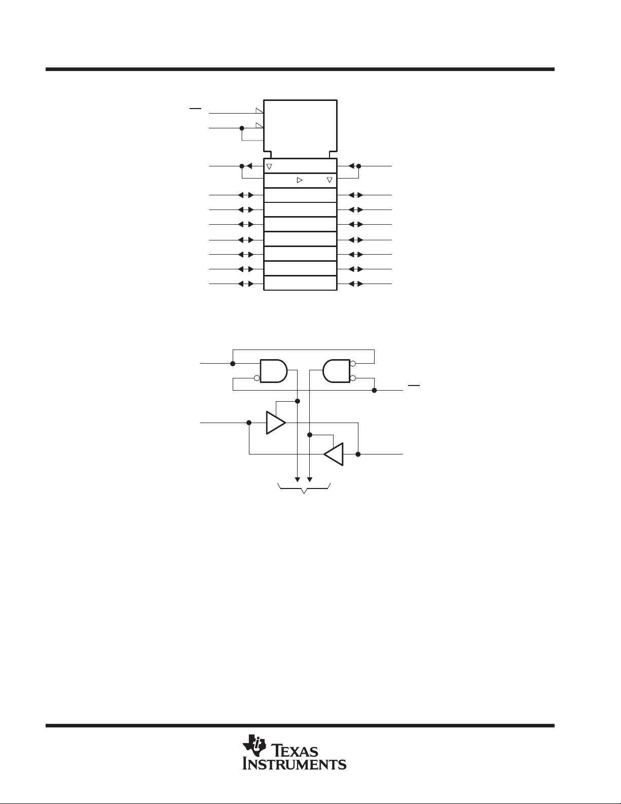
logic symbol
†
This symbol is in accordance with ANSI/IEEE Std 91-1984 and IEC Publication 617-12.
†
OE
DIR
A1
A2
A3
A4
A5
A6
A7
A8
19
1
2
3
4
5
6
7
8
9
G3
3 EN1 [BA]
3 EN2 [AB]
1
2
logic diagram (positive logic)
1
DIR
18
17
16
15
14
13
12
11
B1
B2
B3
B4
B5
B6
B7
B8
A1
19
OE
2
18
B1
To Seven Other Channels
2
POST OFFICE BOX 655303 • DALLAS, TEXAS 75265
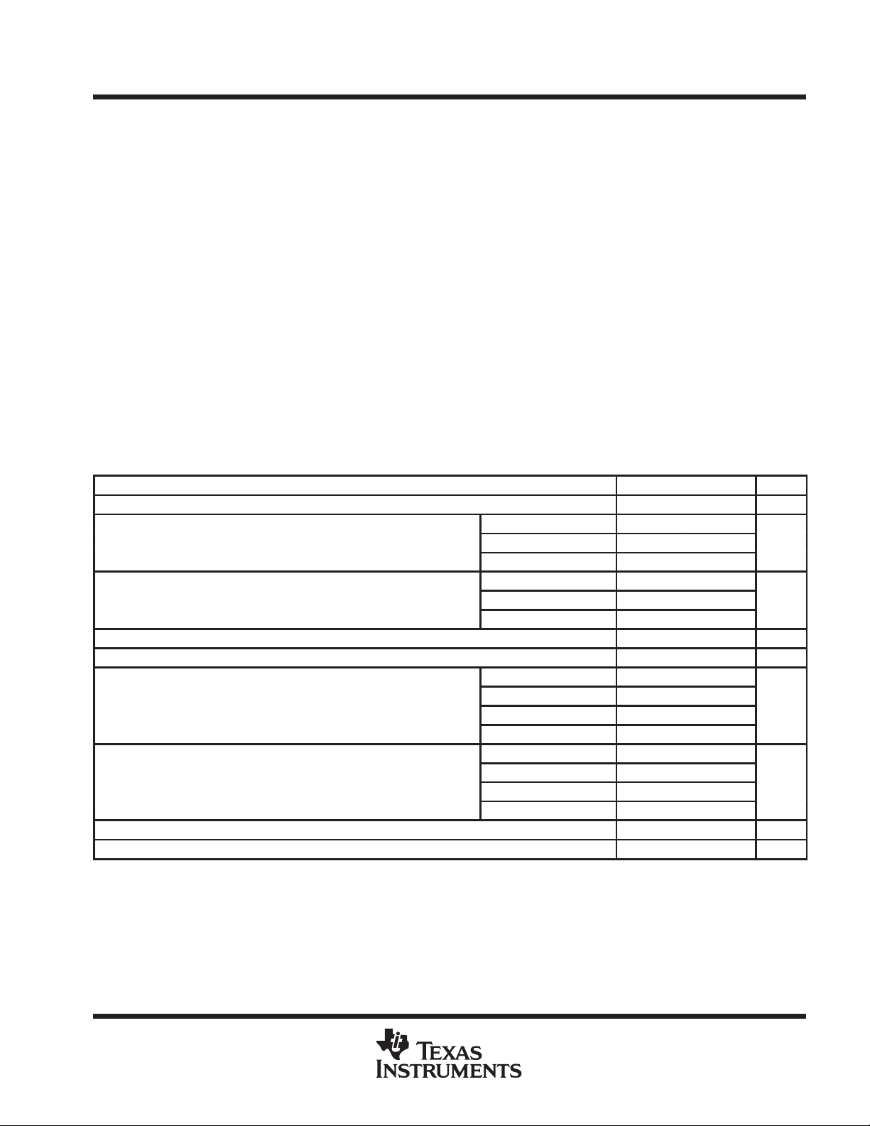
IOHHigh-level output current
mA
IOLLow-level output current
mA
SN74ALVCH245
OCTAL BUS TRANSCEIVER
WITH 3-STATE OUTPUTS
SCES119D – JULY 1997 – REVISED MAY 1999
absolute maximum ratings over operating free-air temperature range (unless otherwise noted)
Supply voltage range, V
Input voltage range, V
Output voltage range, V
Input clamp current, I
Output clamp current, I
Continuous output current, I
Continuous current through V
Package thermal impedance, θ
–0.5 V to 4.6 V. . . . . . . . . . . . . . . . . . . . . . . . . . . . . . . . . . . . . . . . . . . . . . . . . . . . . . . . .
CC
: Except I/O ports (see Note 1) –0.5 V to 4.6 V. . . . . . . . . . . . . . . . . . . . . . . . . . . . . . . . .
I
I/O ports (see Notes 1 and 2) –0.5 V to V
(see Notes 1 and 2) –0.5 V to VCC + 0.5 V. . . . . . . . . . . . . . . . . . . . . . . . . . . . . . . . . .
O
(VI < 0) –50 mA. . . . . . . . . . . . . . . . . . . . . . . . . . . . . . . . . . . . . . . . . . . . . . . . . . . . . . . . . . .
IK
(VO < 0) –50 mA. . . . . . . . . . . . . . . . . . . . . . . . . . . . . . . . . . . . . . . . . . . . . . . . . . . . . . . .
OK
±50 mA. . . . . . . . . . . . . . . . . . . . . . . . . . . . . . . . . . . . . . . . . . . . . . . . . . . . . . . . . . . . .
O
or GND ±100 mA. . . . . . . . . . . . . . . . . . . . . . . . . . . . . . . . . . . . . . . . . . . . . . . . . .
CC
(see Note 3): DGV package 146°C/W. . . . . . . . . . . . . . . . . . . . . . . . . . . . . . .
JA
CC
†
+ 0.5 V. . . . . . . . . . . . . . . . . . . . . . . . . . .
DW package 97°C/W. . . . . . . . . . . . . . . . . . . . . . . . . . . . . . . . .
PW package 128°C/W. . . . . . . . . . . . . . . . . . . . . . . . . . . . . . . .
Storage temperature range, T
†
Stresses beyond those listed under “absolute maximum ratings” may cause permanent damage to the device. These are stress ratings only, and
functional operation of the device at these or any other conditions beyond those indicated under “recommended operating conditions” is not
implied. Exposure to absolute-maximum-rated conditions for extended periods may affect device reliability.
NOTES: 1. The input negative-voltage and output voltage ratings may be exceeded if the input and output current ratings are observed.
2. This value is limited to 4.6 V maximum.
3. The package thermal impedance is calculated in accordance with JESD 51.
–65°C to 150°C. . . . . . . . . . . . . . . . . . . . . . . . . . . . . . . . . . . . . . . . . . . . . . . . . . .
stg
recommended operating conditions (see Note 4)
MIN MAX UNIT
V
V
V
V
V
∆t/∆v Input transition rise or fall rate 10 ns/V
T
NOTE 4: All unused control inputs of the device must be held at VCC or GND to ensure proper device operation. Refer to the TI application report,
Supply voltage 1.65 3.6 V
CC
VCC = 1.65 V to 1.95 V 0.65 × V
High-level input voltage
IH
Low-level input voltage
IL
Input voltage 0 V
I
Output voltage 0 V
O
p
p
Operating free-air temperature –40 85 °C
A
Implications of Slow or Floating CMOS Inputs
, literature number SCBA004.
VCC = 2.3 V to 2.7 V 1.7
VCC = 2.7 V to 3.6 V 2
VCC = 1.65 V to 1.95 V 0.35 × V
VCC = 2.3 V to 2.7 V
VCC = 2.7 V to 3.6 V 0.8
VCC = 1.65 V –4
VCC = 2.3 V –12
VCC = 2.7 V –12
VCC = 3 V –24
VCC = 1.65 V 4
VCC = 2.3 V 12
VCC = 2.7 V 12
VCC = 3 V 24
CC
0.7
CC
CC
V
CC
V
V
V
POST OFFICE BOX 655303 • DALLAS, TEXAS 75265
3
 Loading...