Texas Instruments SN74ALVCH16903DGGR, SN74ALVCH16903DGVR, SN74ALVCH16903DL, SN74ALVCH16903DLR Datasheet

SN74ALVCH16903
3.3-V 12-BIT UNIVERSAL BUS DRIVER
WITH PARITY CHECKER AND DUAL 3-STATE OUTPUTS
SCES095C – MARCH 1997 – REVISED MA Y 1998
D
Member of the Texas Instruments
D
Widebus
EPIC
Family
(Enhanced-Performance Implanted
CMOS) Submicron Process
D
Checks Parity
D
Able to Cascade With a Second
SN74ALVCH16903
D
ESD Protection Exceeds 2000 V Per
MIL-STD-883, Method 3015; Exceeds 200 V
Using Machine Model (C = 200 pF, R = 0)
D
Latch-Up Performance Exceeds 250 mA Per
JESD 17
D
Bus Hold on Data Inputs Eliminates the
Need for External Pullup/Pulldown
Resistors
D
Package Options Include Plastic 300-mil
Shrink Small-Outline (DL), Thin Shrink
Small-Outline (DGG), and Thin Very
Small-Outline (DGV) Packages
description
This 12-bit universal bus driver is designed for
2.3-V to 3.6-V V
The SN74AL VCH16903 has dual outputs and can
operate as a buffer or an edge-triggered register .
In both modes, parity is checked on AP AR, which
arrives one cycle after the data to which it applies.
The YERR
output, which is produced one cycle
after APAR, is open drain.
operation.
CC
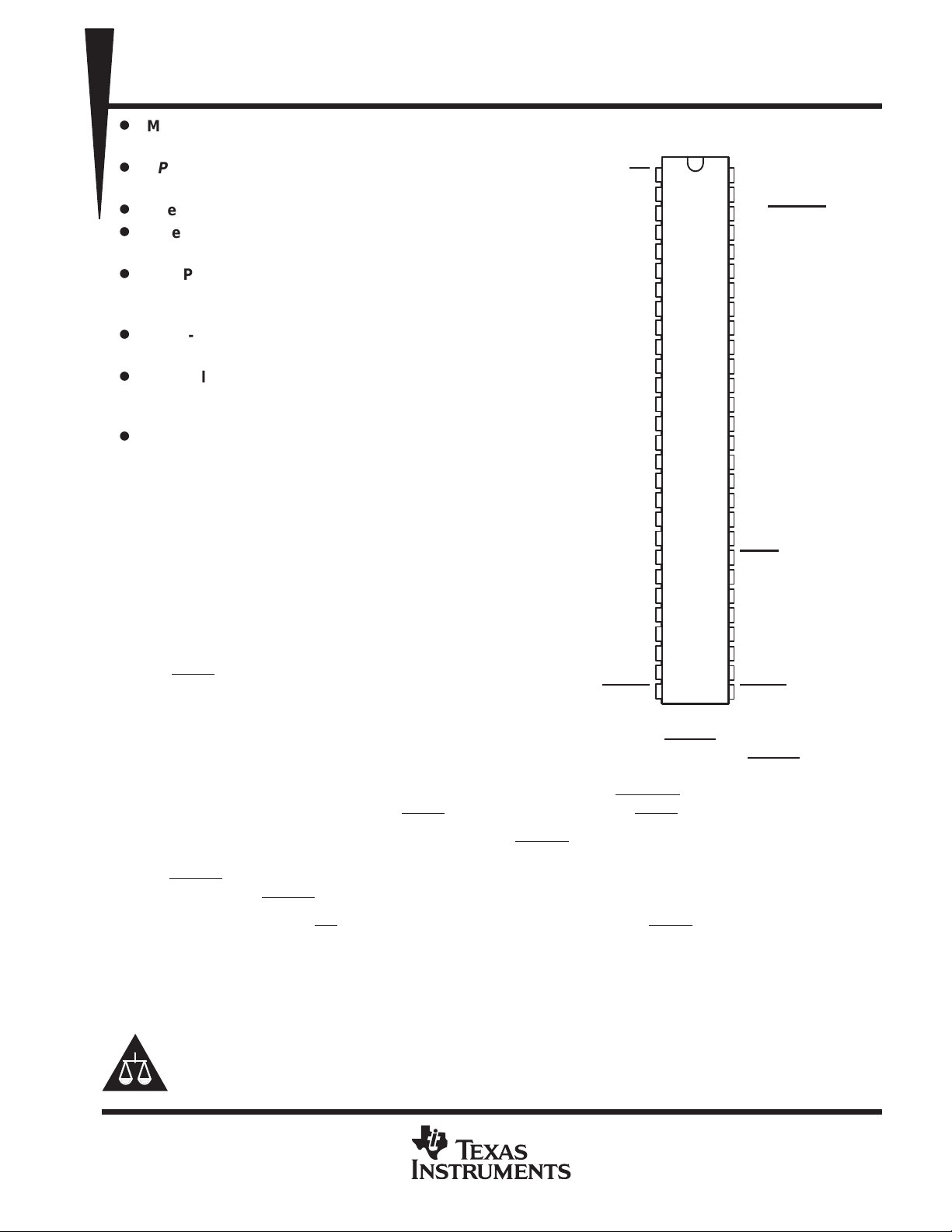
DGG, DGV, OR DL PACKAGE
P AROE
OE
1Y1
1Y2
GND
2Y1
2Y2
V
CC
3Y1
3Y2
4Y1
GND
4Y2
5Y1
5Y2
6Y1
6Y2
7Y1
GND
7Y2
8Y1
8Y2
V
CC
9Y1
9Y2
GND
10Y1
10Y2
(TOP VIEW)
1
56
2
55
3
54
4
53
5
52
6
51
7
50
8
49
9
48
10
47
11
46
12
45
13
44
14
43
15
42
16
41
17
40
18
39
19
38
20
37
21
36
22
35
23
34
24
33
25
32
26
31
27
30
28
29
CLK
1A
1 1A/YERREN
GND
1 1Y1
1 1Y2
V
CC
2A
3A
4A
GND
12A
12Y1
12Y2
5A
6A
7A
GND
APAR
8A
YERR
V
CC
9A
MODE
GND
10A
P ARI/O
CLKEN
MODE selects one of the two data paths. When MODE is low, the device operates as an edge-triggered register .
On the positive transition of the clock (CLK) input and when the clock-enable (CLKEN
) input is low, data set up
at the A inputs is stored in the internal registers. On the positive transition of CLK and when CLKEN
data set up at the 9A–12A inputs is stored in their internal registers. When MODE is high, the device operates
as a buffer and data at the A inputs passes directly to the outputs. 1 1A/YERREN
as a normal data bit and also enables YERR
When used as a single device, parity output enable (PAROE
data to be clocked into the YERR output register.
) must be tied high; when parity input/output
serves a dual purpose; it acts
(PARI/O) is low, even parity is selected and when PARI/O is high, odd parity is selected. When used in pairs
and P AROE
used in pairs and PAROE
A buffered output-enable (OE
is low, the parity sum is output on PARI/O for cascading to the second SN74ALVCH16903. When
is high, PARI/O accepts a partial parity sum from the first SN74AL VCH16903.
) input can be used to place the 24 outputs and YERR in either a normal logic state
(high or low logic levels) or a high-impedance state. In the high-impedance state, the outputs neither load nor
drive the bus lines significantly. The high-impedance state and increased drive provide the capability to drive
bus lines without need for interface or pullup components.
Please be aware that an important notice concerning availability, standard warranty, and use in critical applications of
Texas Instruments semiconductor products and disclaimers thereto appears at the end of this data sheet.
EPIC and Widebus are trademarks of Texas Instruments Incorporated.
PRODUCTION DATA information is current as of publication date.
Products conform to specifications per the terms of Texas Instruments
standard warranty. Production processing does not necessarily include
testing of all parameters.
Copyright 1998, Texas Instruments Incorporated
is high, only
POST OFFICE BOX 655303 • DALLAS, TEXAS 75265
1

SN74ALVCH16903
OUTPUT
3.3-V 12-BIT UNIVERSAL BUS DRIVER
WITH PARITY CHECKER AND DUAL 3-STATE OUTPUTS
SCES095C – MARCH 1997 – REVISED MA Y 1998
description (continued)
OE does not affect the internal operation of the device. Old data can be retained or new data can be entered
while the outputs are in the high-impedance state.
T o ensure the high-impedance state during power up or power down, OE
should be tied to VCC through a pullup
resistor; the minimum value of the resistor is determined by the current-sinking capability of the driver.
Active bus-hold circuitry is provided to hold unused or floating data inputs at a valid logic level.
The SN74ALVCH16903 is characterized for operation from 0°C to 70°C.
Function Tables
FUNCTION
INPUTS
OE MODE CLKEN CLK A 1Y
L L L ↑ H H H
L LL↑LL L
LLH↑HY
LLH↑LY
LHXXH H H
LHXXL L L
HXXXX Z Z
†
n = 1, 2
PARITY FUNCTION
INPUTS
§
OE PAROE‡11A/YERREN
L H L L 0, 2, 4, 6, 8, 10 L H
L H L L 1, 3, 5, 7, 9 L L
L H L L 0, 2, 4, 6, 8, 10 H L
L H L L 1, 3, 5, 7, 9 H H
L H L H 0, 2, 4, 6, 8, 10 L L
L H L H 1, 3, 5, 7, 9 L H
L H L H 0, 2, 4, 6, 8, 10 H H
L H L H 1, 3, 5, 7, 9 H L
H X X X X X H
L X H X X X H
‡
When used as a single device, PAROE must be tied high.
§
Valid after appropriate number of clock pulses have set internal register
PARI/O
Σ OF INPUTS
1A – 10A = H
†
– 8Y
n
0
0
OUTPUTS
†
9Y
n
APAR
†
– 12Y
n
H
L
†
n
YERR
2
POST OFFICE BOX 655303 • DALLAS, TEXAS 75265

OUTPUT
SN74ALVCH16903
3.3-V 12-BIT UNIVERSAL BUS DRIVER
WITH PARITY CHECKER AND DUAL 3-STATE OUTPUTS
SCES095C – MARCH 1997 – REVISED MA Y 1998
Function Tables (Continued)
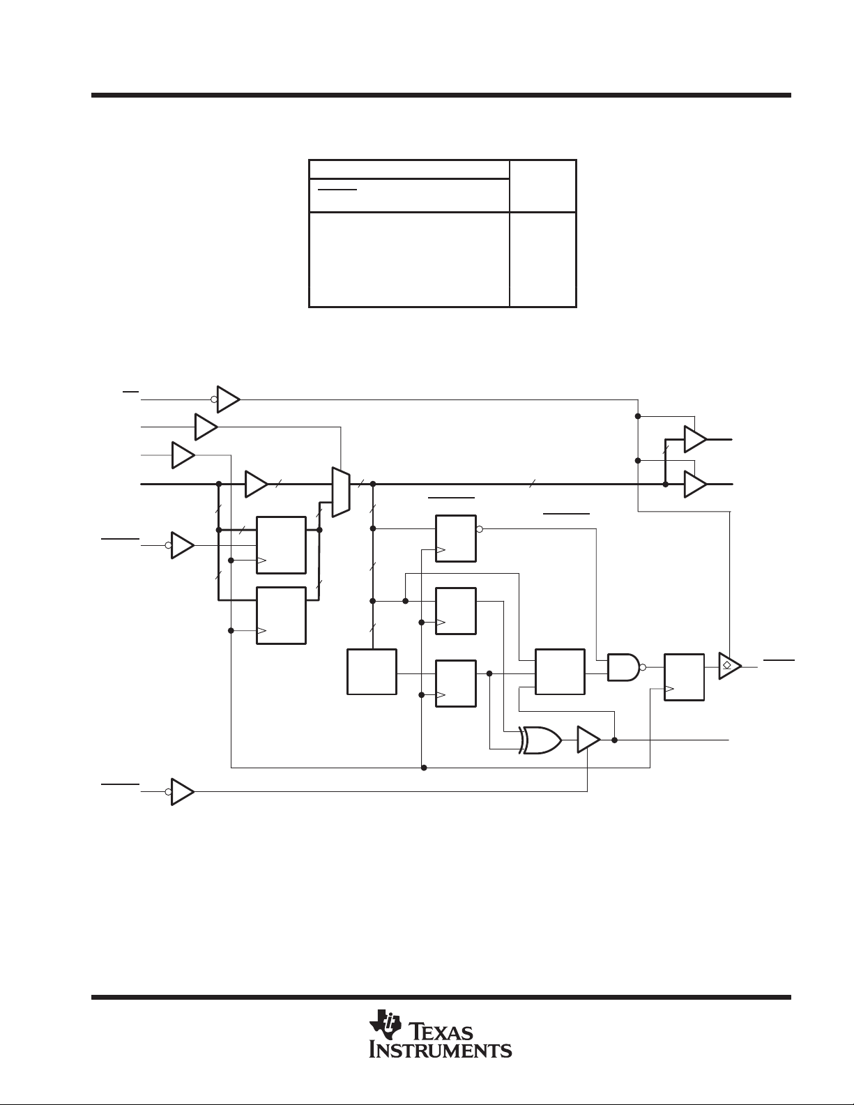
logic diagram (positive logic)
1
OE
33
MODE
56
CLK
1A–12A,
APAR
CLKEN
(9A–12A, APAR)
13
29
5
13
(1A–8A)
8
Flip-Flop
Flip-Flop
PARI/O FUNCTION
INPUTS
PAROE
L 0, 2, 4, 6, 8, 10 L L
L 1, 3, 5, 7, 9 L H
L 0, 2, 4, 6, 8, 10 H H
L 1, 3, 5, 7, 9 H L
H X X Z
†
This table applies to the first device of a cascaded pair
of ALVCH16903 devices.
13
5
(1A–10A)
Σ OF INPUTS
1A – 10A = H
13
(1A–11A/YERREN
12
11
APAR
10
Parity
Check
DQ
DQ
DQ
†
APAR
, APAR)
APAR
PARI/O
(1A–12A)
12
11A/YERREN
XOR
12
DQ
1Y1–12Y1
1Y2–12Y2
36
YERR
PAROE
28
POST OFFICE BOX 655303 • DALLAS, TEXAS 75265
30
PARI/O
3

SN74ALVCH16903
VIHHigh-level input voltage
V
VILLow-level input voltage
V
Y port
IOHHigh-level output current
mA
V
V
Y port
3.3-V 12-BIT UNIVERSAL BUS DRIVER
WITH PARITY CHECKER AND DUAL 3-STATE OUTPUTS
SCES095C – MARCH 1997 – REVISED MA Y 1998
absolute maximum ratings over operating free-air temperature range (unless otherwise noted)
Supply voltage range, V
Input voltage range, V
Output voltage range, V
Input clamp current, I
Output clamp current, I
Continuous output current, I
Continuous current through each V
Package thermal impedance, θ
–0.5 V to 4.6 V. . . . . . . . . . . . . . . . . . . . . . . . . . . . . . . . . . . . . . . . . . . . . . . . . . . . . . . . .
CC
(see Note 1) –0.5 V to 4.6 V. . . . . . . . . . . . . . . . . . . . . . . . . . . . . . . . . . . . . . . . . . . . . . . . .
I
(see Notes 1 and 2) –0.5 V to VCC + 0.5 V. . . . . . . . . . . . . . . . . . . . . . . . . . . . . . . . . .
O
(VI < 0) –50 mA. . . . . . . . . . . . . . . . . . . . . . . . . . . . . . . . . . . . . . . . . . . . . . . . . . . . . . . . . . .
IK
(VO < 0) –50 mA. . . . . . . . . . . . . . . . . . . . . . . . . . . . . . . . . . . . . . . . . . . . . . . . . . . . . . . .
OK
±50 mA. . . . . . . . . . . . . . . . . . . . . . . . . . . . . . . . . . . . . . . . . . . . . . . . . . . . . . . . . . . . .
O
JA
or GND ±100 mA. . . . . . . . . . . . . . . . . . . . . . . . . . . . . . . . . . . . . . . . . . . . .
CC
(see Note 3): DGG package 81°C/W. . . . . . . . . . . . . . . . . . . . . . . . . . . . . . . .
†
DGV package 86°C/W. . . . . . . . . . . . . . . . . . . . . . . . . . . . . . . .
DL package 74°C/W. . . . . . . . . . . . . . . . . . . . . . . . . . . . . . . . . .
Storage temperature range, T
†
Stresses beyond those listed under “absolute maximum ratings” may cause permanent damage to the device. These are stress ratings only, and
functional operation of the device at these or any other conditions beyond those indicated under “recommended operating conditions” is not
implied. Exposure to absolute-maximum-rated conditions for extended periods may affect device reliability.
NOTES: 1. The input negative-voltage and output voltage ratings may be exceeded if the input and output current ratings are observed.
2. This value is limited to 4.6 V maximum.
3. The package thermal impedance is calculated in accordance with JESD 51.
–65°C to 150°C. . . . . . . . . . . . . . . . . . . . . . . . . . . . . . . . . . . . . . . . . . . . . . . . . . .
stg
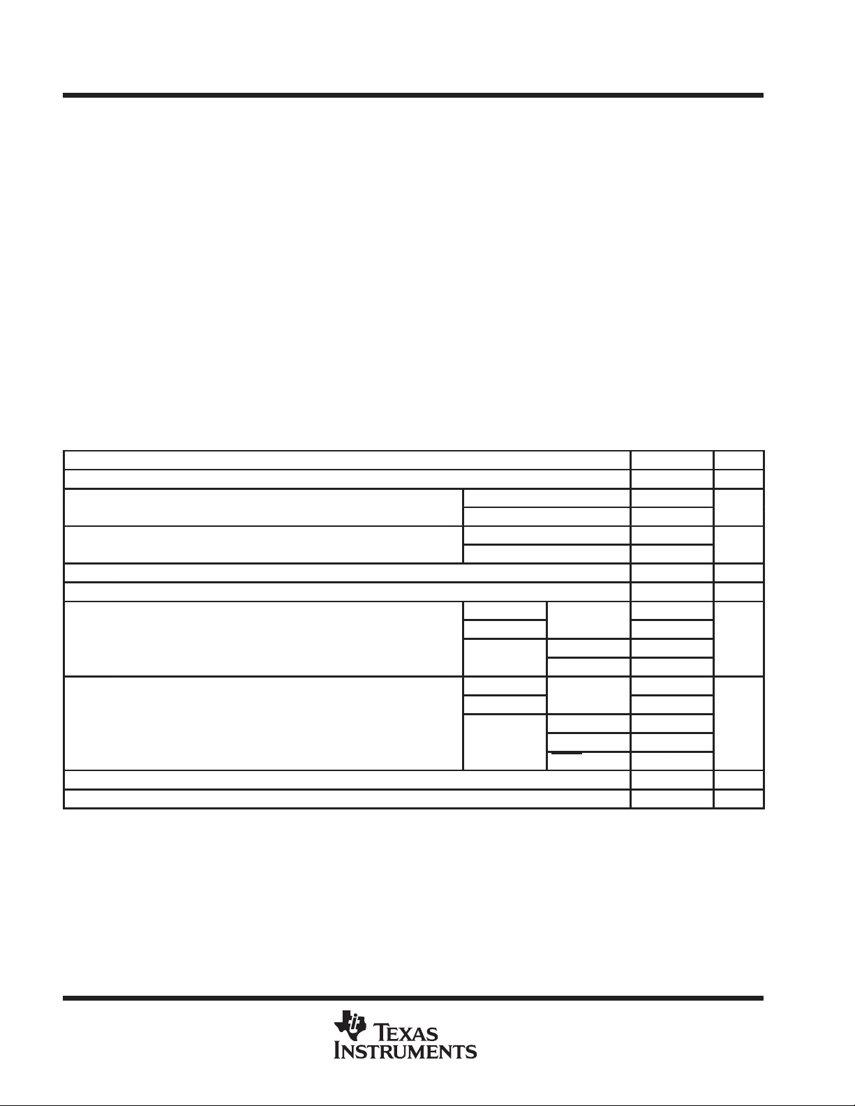
recommended operating conditions (see Note 4)
MIN MAX UNIT
V
V
V
I
OL
∆t/∆v Input transition rise or fall rate 0 10 ns/V
T
NOTE 4: All unused control inputs of the device must be held at VCC or GND to ensure proper device operation. Refer to the TI application report,
Supply voltage 2.3 3.6 V
CC
p
p
Input voltage 0 V
I
Output voltage 0 V
O
p
Low-level output current
Operating free-air temperature 0 70 °C
A
Implications of Slow or Floating CMOS Inputs
, literature number SCBA004.
VCC = 2.3 V to 2.7 V 1.7
VCC = 2.7 V to 3.6 V 2
VCC = 2.3 V to 2.7 V 0.7
VCC = 2.7 V to 3.6 V 0.8
VCC = 2.3 V
VCC = 2.7 V
= 3
CC
VCC = 2.3 V
VCC = 2.7 V
VCC = 3 V
p
PARI/O –12
Y port –24
p
PARI/O 12
Y port 24
YERR output 24
CC
CC
–12
–12
12
12
V
V
mA
4
POST OFFICE BOX 655303 • DALLAS, TEXAS 75265
 Loading...