

SN74ALVCH16901
18-BIT UNIVERSAL BUS TRANSCEIVER
WITH PARITY GENERATORS/CHECKERS
SCES010E – JULY 1995 – REVISED FEBRUARY 1999
1
POST OFFICE BOX 655303 • DALLAS, TEXAS 75265
D
Member of the Texas Instruments
Widebus+
Family
D
EPIC
(Enhanced-Performance Implanted
CMOS) Submicron Process
D
UBT
(Universal Bus Transceiver)
Combines D-Type Latches and D-Type
Flip-Flops for Operation in Transparent,
Latched, or Clocked Mode
D
Simultaneously Generates and Checks
Parity
D
Option to Select Generate Parity and Check
or Feed-Through Data/Parity in A-to-B or
B-to-A Directions
D
ESD Protection Exceeds 2000 V Per
MIL-STD-883, Method 3015; Exceeds 200 V
Using Machine Model (C = 200 pF, R = 0)
D
Latch-Up Performance Exceeds 250 mA Per
JESD 17
D
Bus Hold on Data Inputs Eliminates the
Need for External Pullup/Pulldown
Resistors
D
Packaged in Thin Shrink Small-Outline
Package
description
This 18-bit (dual-octal) noninverting registered
transceiver is designed for 1.65-V to 3.6-V V
CC
operation.
The SN74AL VCH16901 is a dual 9-bit to dual 9-bit
parity transceiver with registers. The device can
operate as a feed-through transceiver or it can
generate/check parity from the two 8-bit data
buses in either direction.
The SN74ALVCH16901 features independent clock (CLKAB or CLKBA), latch-enable (LEAB or LEBA), and
dual 9-bit clock-enable (CLKENAB
or CLKENBA) inputs. It also provides parity-enable (SEL) and parity-select
(ODD/EVEN
) inputs and separate error-signal (ERRA or ERRB) outputs for checking parity. The direction of
data flow is controlled by OEAB
and OEBA. When SEL is low, the parity functions are enabled. When SEL is
high, the parity functions are disabled and the device acts as an 18-bit registered transceiver.
T o ensure the high-impedance state during power up or power down, OE
should be tied to VCC through a pullup
resistor; the minimum value of the resistor is determined by the current-sinking capability of the driver.
Active bus-hold circuitry is provided to hold unused or floating data inputs at a valid logic level.
The SN74ALVCH16901 is characterized for operation from –40°C to 85°C.
Copyright 1999, Texas Instruments Incorporated
PRODUCTION DATA information is current as of publication date.
Products conform to specifications per the terms of Texas Instruments
standard warranty. Production processing does not necessarily include
testing of all parameters.
Please be aware that an important notice concerning availability, standard warranty, and use in critical applications of
Texas Instruments semiconductor products and disclaimers thereto appears at the end of this data sheet.
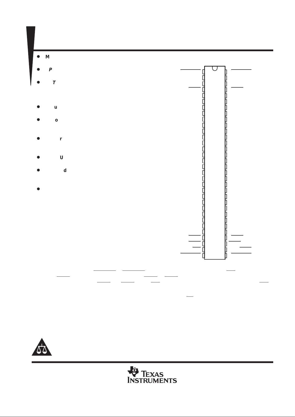
DGG PACKAGE
(TOP VIEW)
1
2
3
4
5
6
7
8
9
10
11
12
13
14
15
16
17
18
19
20
21
22
23
24
25
26
27
28
29
30
31
32
64
63
62
61
60
59
58
57
56
55
54
53
52
51
50
49
48
47
46
45
44
43
42
41
40
39
38
37
36
35
34
33
1CLKENAB
LEAB
CLKAB
1ERRA
1APAR
GND
1A1
1A2
1A3
V
CC
1A4
1A5
1A6
GND
1A7
1A8
2A1
2A2
GND
2A3
2A4
2A5
V
CC
2A6
2A7
2A8
GND
2APAR
2ERRA
OEAB
SEL
2CLKENAB
1CLKENBA
LEBA
CLKBA
1ERRB
1BPAR
GND
1B1
1B2
1B3
V
CC
1B4
1B5
1B6
GND
1B7
1B8
2B1
2B2
GND
2B3
2B4
2B5
V
CC
2B6
2B7
2B8
GND
2BPAR
2ERRB
OEBA
ODD/EVEN
2CLKENBA
Widebus+, EPIC, and UBT are trademarks of Texas Instruments Incorporated.
SN74ALVCH16901
18-BIT UNIVERSAL BUS TRANSCEIVER
WITH PARITY GENERATORS/CHECKERS
SCES010E – JULY 1995 – REVISED FEBRUARY 1999
2
POST OFFICE BOX 655303 • DALLAS, TEXAS 75265
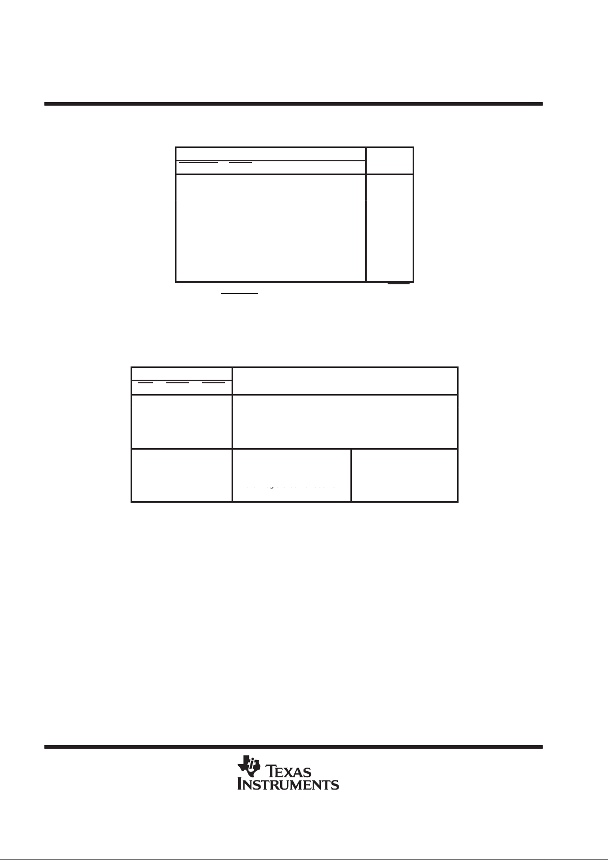
Function Tables
FUNCTION
†
INPUTS
OUTPUT
CLKENAB OEAB LEAB CLKAB A
B
X H X X X Z
X LH XL L
X LH XH H
H LL XXB
0
‡
L LL ↑LL
L LL ↑HH
L LL LXB
0
‡
L LL HXB
0
§
†
A-to-B data flow is shown: B-to-A flow is similar, but uses OEBA,
LEBA, and CLKENBA
.
‡
Output level before the indicated steady-state input conditions were
established
§
Output level before the indicated steady-state input conditions were
established, provided that CLKAB was low before LEAB went low
PARITY ENABLE
INPUTS
SEL OEBA OEAB
OPERATION OR FUNCTION
L H L Parity is checked on port A and is generated on port B.
L L H Parity is checked on port B and is generated on port A.
L H H Parity is checked on port B and port A.
L L L Parity is generated on port A and B if device is in FF mode.
H L L QA data to B, QB data to A
H LH
Parity functions are disabled;
QB data to A
H HL
device
acts
as
a
standard
18-bit registered transceiver.
QA data to B
H H H
18 bit registered transceiver.
Isolation

SN74ALVCH16901
18-BIT UNIVERSAL BUS TRANSCEIVER
WITH PARITY GENERATORS/CHECKERS
SCES010E – JULY 1995 – REVISED FEBRUARY 1999
3
POST OFFICE BOX 655303 • DALLAS, TEXAS 75265
Function Tables (Continued)
PARITY
INPUTS
OUTPUTS
SEL OEBA OEAB ODD/EVEN
Σ OF INPUTS
A1–A8 = H
Σ OF INPUTS
B1–B8 = H
APAR BPAR APAR
ERRA
BPAR
ERRB
L H L L 0, 2, 4, 6, 8 N/A L N/A N/A H L Z
L H L L 1, 3, 5, 7 N/A L N/A N/A LHZ
LH L L 0, 2, 4, 6, 8 N/A H N/A N/A LLZ
LH L L 1, 3, 5, 7 N/A H N/A N/A HHZ
LLH L N/A 0, 2, 4, 6, 8 N/A L L Z N/A H
L L H L N/A 1, 3, 5, 7 N/A L H Z N/A L
L L H L N/A 0, 2, 4, 6, 8 N/A H L Z N/A L
L L H L N/A 1, 3, 5, 7 N/A H H Z N/A H
L H L H 0, 2, 4, 6, 8 N/A L N/A N/A L H Z
L H L H 1, 3, 5, 7 N/A L N/A N/A HLZ
LH L H 0, 2, 4, 6, 8 N/A H N/A N/A HHZ
LH L H 1, 3, 5, 7 N/A H N/A N/A LLZ
LLH H N/A 0, 2, 4, 6, 8 N/A L H Z N/A L
L L H H N/A 1, 3, 5, 7 N/A L L Z N/A H
L L H H N/A 0, 2, 4, 6, 8 N/A H H Z N/A H
L L H H N/A 1, 3, 5, 7 N/A H L Z N/A L
L H H L 0, 2, 4, 6, 8 0, 2, 4, 6, 8 L L Z H Z H
L H H L 1, 3, 5, 7 1, 3, 5, 7 L L Z LZL
LH H L 0, 2, 4, 6, 8 0, 2, 4, 6, 8 H H Z LZL
LH H L 1, 3, 5, 7 1, 3, 5, 7 H H Z HZH
LHH H 0, 2, 4, 6, 8 0, 2, 4, 6, 8 L L Z L Z L
L H H H 1, 3, 5, 7 1, 3, 5, 7 L L Z HZH
LH H H 0, 2, 4, 6, 8 0, 2, 4, 6, 8 H H Z HZH
LH H H 1, 3, 5, 7 1, 3, 5, 7 H H Z LZL
LLL L N/A N/A N/A N/A PE
†
Z PE
†
Z
L L L H N/A N/A N/A N/A PO
‡
Z PO
‡
Z
†
Parity output is set to the level so that the specific bus side is set to even parity.
‡
Parity output is set to the level so that the specific bus side is set to odd parity.
SN74ALVCH16901
18-BIT UNIVERSAL BUS TRANSCEIVER
WITH PARITY GENERATORS/CHECKERS
SCES010E – JULY 1995 – REVISED FEBRUARY 1999
4
POST OFFICE BOX 655303 • DALLAS, TEXAS 75265
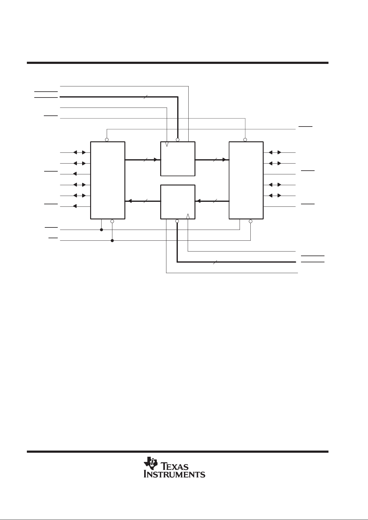
functional block diagram
A-Port
Parity
Generate
and
Check
B Data
B-Port
Parity
Generate
and
Check
A Data
18-Bit
Storage
18-Bit
Storage
18 18
1818
2
2
LEAB
1CLKENAB
2CLKENAB
CLKAB
OEAB
1A1–1A8
1APAR
1ERRB
2A1–2A8
2APAR
2ERRB
ODD/EVEN
SEL
OEBA
1B1–1B8
1BPAR
1ERRA
2B1–2B8
2BPAR
2ERRA
1CLKENBA
2CLKENBA
CLKBA
LEBA
Q
A
Q
B
5
61
28
36
34
31
35
60
4
37
29
62
64, 33
63
2
1, 32
3
30
absolute maximum ratings over operating free-air temperature range (unless otherwise noted)
†
Supply voltage range, V
CC
–0.5 V to 4.6 V. . . . . . . . . . . . . . . . . . . . . . . . . . . . . . . . . . . . . . . . . . . . . . . . . . . . . . . . .
Input voltage range, V
I
: Except I/O ports (see Note 1) –0.5 V to 4.6 V. . . . . . . . . . . . . . . . . . . . . . . . . . . . . . . . .
I/O ports (see Notes 1 and 2 –0.5 V to V
CC
+ 0.5 V. . . . . . . . . . . . . . . . . . . . . . . . . . . .
Output voltage range, V
O
(see Notes 1 and 2) –0.5 V to VCC + 0.5 V. . . . . . . . . . . . . . . . . . . . . . . . . . . . . . . . . .
Input clamp current, I
IK
(VI < 0) –50 mA. . . . . . . . . . . . . . . . . . . . . . . . . . . . . . . . . . . . . . . . . . . . . . . . . . . . . . . . . . .
Output clamp current, I
OK
(VO < 0) –50 mA. . . . . . . . . . . . . . . . . . . . . . . . . . . . . . . . . . . . . . . . . . . . . . . . . . . . . . . .
Continuous output current, I
O
±50 mA. . . . . . . . . . . . . . . . . . . . . . . . . . . . . . . . . . . . . . . . . . . . . . . . . . . . . . . . . . . . .
Continuous current through each V
CC
or GND ±100 mA. . . . . . . . . . . . . . . . . . . . . . . . . . . . . . . . . . . . . . . . . . . . .
Package thermal impedance, θ
JA
(see Note 3) 73°C/W. . . . . . . . . . . . . . . . . . . . . . . . . . . . . . . . . . . . . . . . . . . . .
Storage temperature range, T
stg
–65°C to 150°C. . . . . . . . . . . . . . . . . . . . . . . . . . . . . . . . . . . . . . . . . . . . . . . . . . .
†
Stresses beyond those listed under “absolute maximum ratings” may cause permanent damage to the device. These are stress ratings only, and
functional operation of the device at these or any other conditions beyond those indicated under “recommended operating conditions” is not
implied. Exposure to absolute-maximum-rated conditions for extended periods may affect device reliability.
NOTES: 1. The input negative-voltage and output voltage ratings may be exceeded if the input and output current ratings are observed..
2. This value is limited to 4.6 V maximum.
3. The package thermal impedance is calculated in accordance with JESD 51.
 Loading...