

SN74ALVCH16836
20-BIT UNIVERSAL BUS DRIVER
WITH 3-STATE OUTPUTS
SCES089C – OCTOBER 1996 – REVISED FEBRUARY 1999
1
POST OFFICE BOX 655303 • DALLAS, TEXAS 75265
D
Member of the Texas Instruments
Widebus
Family
D
EPIC
(Enhanced-Performance Implanted
CMOS) Submicron Process
D
Designed to Comply With JEDEC 168-Pin
and 200-Pin SDRAM Buffered DIMM
Specification
D
Bus Hold on Data Inputs Eliminates the
Need for External Pullup/Pulldown
Resistors
D
Package Options Include Plastic Shrink
Small-Outline (DL) and Thin Shrink
Small-Outline (DGG) Packages
description
This 20-bit universal bus driver is designed for
1.65-V to 3.6-V V
CC
operation.
Data flow from A to Y is controlled by the
output-enable (OE
) input. The device operates in
the transparent mode when the latch-enable (LE
)
input is low. The A data is latched if the clock (CLK)
input is held at a high or low logic level. If LE
is
high, the A data is stored in the latch/flip-flop on
the low-to-high transition of CLK. When OE
is
high, the outputs are in the high-impedance state.
T o ensure the high-impedance state during power
up or power down, OE
should be tied to V
CC
through a pullup resistor; the minimum value of
the resistor is determined by the current-sinking
capability of the driver.
Active bus-hold circuitry is provided to hold
unused or floating data inputs at a valid logic level.
The SN74ALVCH16836 is characterized for
operation from –40°C to 85°C.
PRODUCT PREVIEW
Copyright 1999, Texas Instruments Incorporated
Please be aware that an important notice concerning availability, standard warranty, and use in critical applications of
Texas Instruments semiconductor products and disclaimers thereto appears at the end of this data sheet.
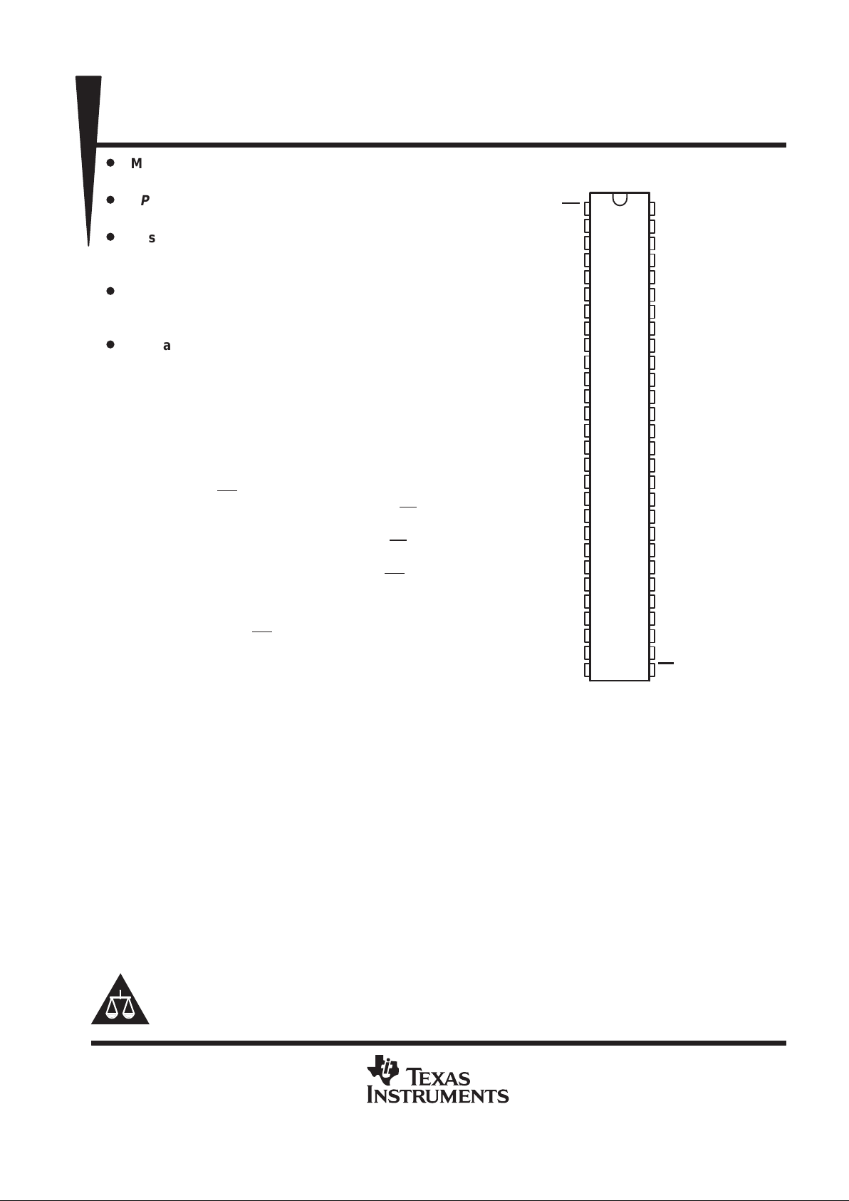
DGG OR DL PACKAGE
(TOP VIEW)
1
2
3
4
5
6
7
8
9
10
11
12
13
14
15
16
17
18
19
20
21
22
23
24
25
26
27
28
56
55
54
53
52
51
50
49
48
47
46
45
44
43
42
41
40
39
38
37
36
35
34
33
32
31
30
29
OE
Y1
Y2
GND
Y3
Y4
V
CC
Y5
Y6
Y7
GND
Y8
Y9
Y10
Y1 1
Y12
Y13
GND
Y14
Y15
Y16
V
CC
Y17
Y18
GND
Y19
Y20
NC
CLK
A1
A2
GND
A3
A4
V
CC
A5
A6
A7
GND
A8
A9
A10
A1 1
A12
A13
GND
A14
A15
A16
V
CC
A17
A18
GND
A19
A20
LE
NC – No internal connection
EPIC and Widebus are trademarks of Texas Instruments Incorporated.
PRODUCT PREVIEW information concerns products in the formative or
design phase of development. Characteristic data and other
specifications are design goals. Texas Instruments reserves the right to
change or discontinue these products without notice.
SN74ALVCH16836
20-BIT UNIVERSAL BUS DRIVER
WITH 3-STATE OUTPUTS
SCES089C – OCTOBER 1996 – REVISED FEBRUARY 1999
2
POST OFFICE BOX 655303 • DALLAS, TEXAS 75265
FUNCTION TABLE
INPUTS
OUTPUT
OE LE CLK A
Y
H X X X Z
L LXL L
LLXH H
LH↑LL
LH↑HH
LHHX Y
0
†
LHLX Y
0
‡
†
Output level before the indicated steady-state
input conditions were established, provided
that CLK is high before LE
goes low
‡
Output level before the indicated steady-state
input conditions were established
logic symbol
§
A1
55
A2
54
A3
52
A4
51
A5
49
A6
48
A7
47
A8
45
A9
44
A10
43
A11
42
A12
41
A13
40
A14
38
A15
37
A16
36
A17
34
A18
33
OE
EN1
1
56
CLK
2
Y1
3
Y2
5
Y3
1
6
Y4
8
Y5
9
Y6
10
Y7
12
Y8
13
Y9
14
Y10
15
Y11
16
Y12
17
Y13
19
Y14
20
Y15
21
Y16
23
Y17
24
Y18
C3
29
G2
LE
2C3
13D
A19
31
A20
30
26
Y19
27
Y20
§
This symbol is in accordance with ANSI/IEEE Std 91-1984 and IEC Publication 617-12.
PRODUCT PREVIEW
SN74ALVCH16836
20-BIT UNIVERSAL BUS DRIVER
WITH 3-STATE OUTPUTS
SCES089C – OCTOBER 1996 – REVISED FEBRUARY 1999
3
POST OFFICE BOX 655303 • DALLAS, TEXAS 75265
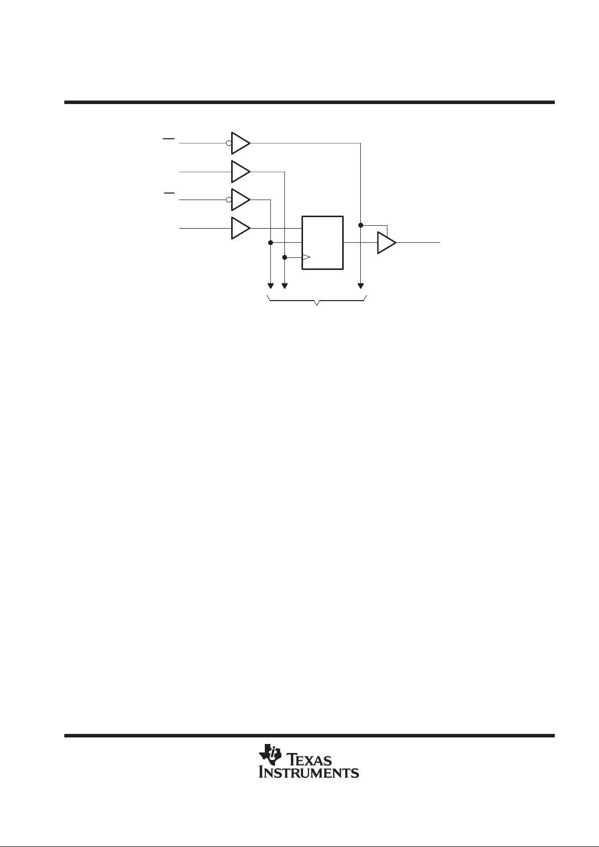
logic diagram (positive logic)
1
56
29
55
1D
C1
CLK
2
To 19 Other Channels
OE
CLK
LE
A1
Y1
absolute maximum ratings over operating free-air temperature range (unless otherwise noted)
†
Supply voltage range, V
CC
–0.5 V to 4.6 V. . . . . . . . . . . . . . . . . . . . . . . . . . . . . . . . . . . . . . . . . . . . . . . . . . . . . . . . .
Input voltage range, V
I
(see Note 1) –0.5 V to 4.6 V. . . . . . . . . . . . . . . . . . . . . . . . . . . . . . . . . . . . . . . . . . . . . . . . .
Output voltage range, V
O
(see Notes 1 and 2) –0.5 V to VCC + 0.5 V. . . . . . . . . . . . . . . . . . . . . . . . . . . . . . . . . .
Input clamp current, I
IK
(VI < 0) –50 mA. . . . . . . . . . . . . . . . . . . . . . . . . . . . . . . . . . . . . . . . . . . . . . . . . . . . . . . . . . .
Output clamp current, I
OK
(VO < 0) –50 mA. . . . . . . . . . . . . . . . . . . . . . . . . . . . . . . . . . . . . . . . . . . . . . . . . . . . . . . .
Continuous output current, I
O
±50 mA. . . . . . . . . . . . . . . . . . . . . . . . . . . . . . . . . . . . . . . . . . . . . . . . . . . . . . . . . . . . .
Continuous current through each V
CC
or GND ±100 mA. . . . . . . . . . . . . . . . . . . . . . . . . . . . . . . . . . . . . . . . . . . . .
Package thermal impedance, θ
JA
(see Note 3): DGG package 81°C/W. . . . . . . . . . . . . . . . . . . . . . . . . . . . . . . .
DL package 74°C/W. . . . . . . . . . . . . . . . . . . . . . . . . . . . . . . . . .
Storage temperature range, T
stg
–65°C to 150°C. . . . . . . . . . . . . . . . . . . . . . . . . . . . . . . . . . . . . . . . . . . . . . . . . . .
†
Stresses beyond those listed under “absolute maximum ratings” may cause permanent damage to the device. These are stress ratings only, and
functional operation of the device at these or any other conditions beyond those indicated under “recommended operating conditions” is not
implied. Exposure to absolute-maximum-rated conditions for extended periods may affect device reliability.
NOTES: 1. The input negative-voltage and output voltage ratings may be exceeded if the input and output current ratings are observed.
2. This value is limited to 4.6 V maximum.
3. The package thermal impedance is calculated in accordance with JESD 51.
PRODUCT PREVIEW
 Loading...