

SN74ALVCH16831
1-TO-4 ADDRESS REGISTER/DRIVER
WITH 3-STATE OUTPUTS
SCES083D – AUGUST 1996 – REVISED FEBRUARY 1999
D
Member of the Texas Instruments
D
Widebus
EPIC
Family
(Enhanced-Performance Implanted
CMOS) Submicron Process
D
ESD Protection Exceeds 2000 V Per
MIL-STD-883, Method 3015; Exceeds 200 V
Using Machine Model (C = 200 pF, R = 0)
D
Latch-Up Performance Exceeds 250 mA Per
JESD 17
D
Bus Hold on Data Inputs Eliminates the
Need for External Pullup/Pulldown
Resistors
D
Packaged in Thin Very Small-Outline
Package
description
This 1-bit to 4-bit address register/driver is
designed for 1.65-V to 3.6-V V
device is ideal for use in applications in which a
single address bus is driving four separate
memory locations. The SN74ALVCH16831 can
be used as a buffer or a register , depending on the
logic level of the select (SEL
When SEL
is logic high, the device is in the buffer
mode. The outputs follow the inputs and are
controlled by the two output-enable (OE
Each OE
When SEL
controls two groups of nine outputs.
is logic low, the device is in the register
mode. The register is an edge-triggered D-type
flip-flop. On the positive transition of the clock
(CLK) input, data set up at the A inputs is stored
in the internal registers. OE
same as in buffer mode.
When OE
is logic low, the outputs are in a normal
logic state (high or low logic level). When OE
logic high, the outputs are in the high-impedance
state.
SEL
and OE do not affect the internal operation of
the flip-flops. Old data can be retained or new data
can be entered while the outputs are in the
high-impedance state.
operation. The
CC
) input.
controls operate the
) controls.
is
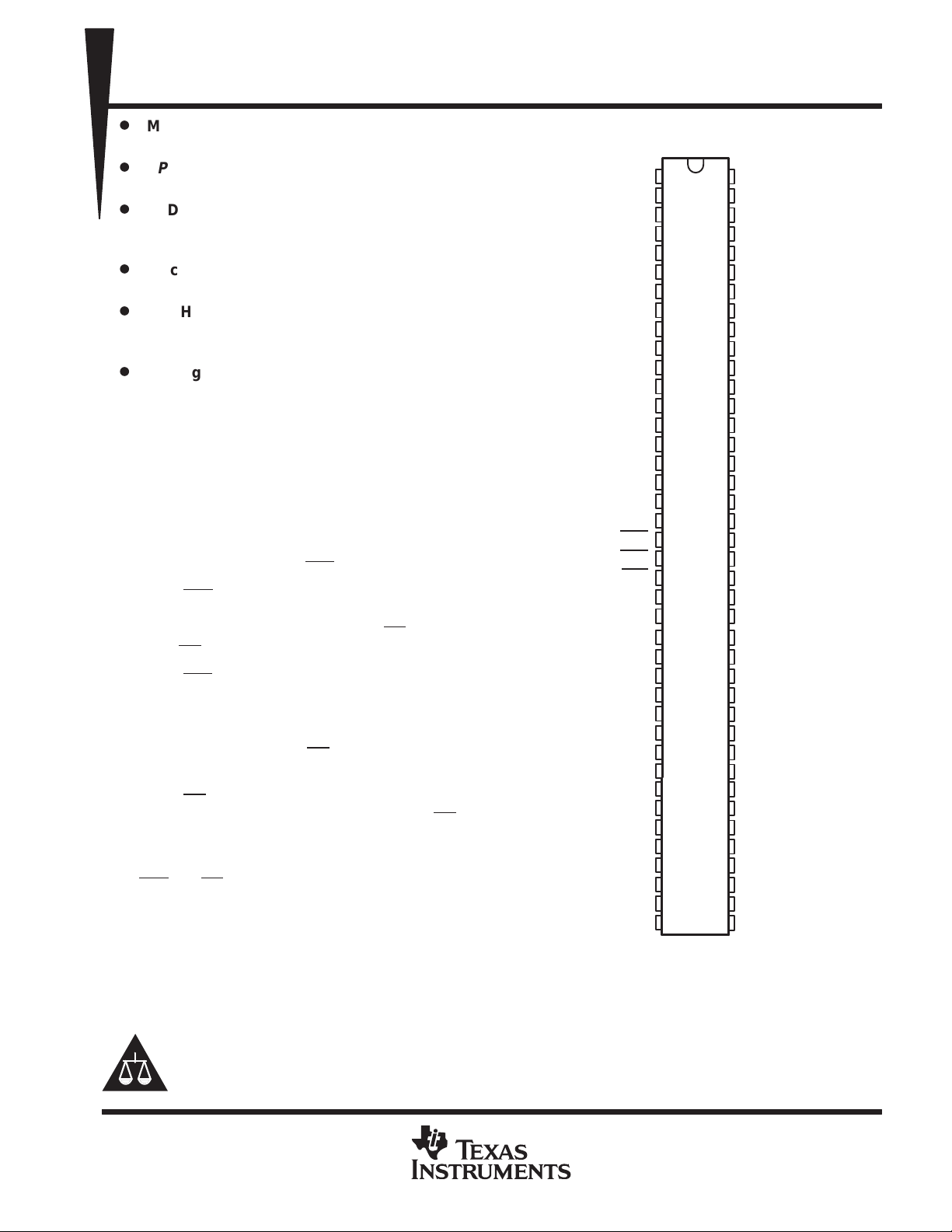
DBB PACKAGE
(TOP VIEW)
4Y1
1
3Y1
2
GND
V
GND
GND
V
GND
CLK
OE1
OE2
SEL
GND
V
GND
GND
V
GND
NC – No internal connection
2Y1
1Y1
CC
NC
A1
NC
A2
NC
A3
CC
NC
A4
A5
A6
CC
A7
NC
A8
NC
A9
NC
CC
4Y9
3Y9
2Y9
1Y9
3
4
5
6
7
8
9
10
11
12
13
14
15
16
17
18
19
20
21
22
23
24
25
26
27
28
29
30
31
32
33
34
35
36
37
38
39
40
80
79
78
77
76
75
74
73
72
71
70
69
68
67
66
65
64
63
62
61
60
59
58
57
56
55
54
53
52
51
50
49
48
47
46
45
44
43
42
41
1Y2
2Y2
GND
3Y2
4Y2
V
CC
1Y3
2Y3
GND
3Y3
4Y3
GND
1Y4
2Y4
V
CC
3Y4
4Y4
GND
1Y5
2Y5
3Y5
4Y5
GND
1Y6
2Y6
V
CC
3Y6
4Y6
GND
1Y7
2Y7
GND
3Y7
4Y7
V
CC
1Y8
2Y8
GND
3Y8
4Y8
Please be aware that an important notice concerning availability, standard warranty, and use in critical applications of
Texas Instruments semiconductor products and disclaimers thereto appears at the end of this data sheet.
EPIC and Widebus are trademarks of Texas Instruments Incorporated.
PRODUCTION DATA information is current as of publication date.
Products conform to specifications per the terms of Texas Instruments
standard warranty. Production processing does not necessarily include
testing of all parameters.
POST OFFICE BOX 655303 • DALLAS, TEXAS 75265
Copyright 1999, Texas Instruments Incorporated
1
SN74ALVCH16831
1-TO-4 ADDRESS REGISTER/DRIVER
WITH 3-STATE OUTPUTS
SCES083D – AUGUST 1996 – REVISED FEBRUARY 1999
description (continued)
T o ensure the high-impedance state during power up or power down, OE should be tied to VCC through a pullup
resistor; the minimum value of the resistor is determined by the current-sinking capability of the driver.
Active bus-hold circuitry is provided to hold unused or floating data inputs at a valid logic level.
The SN74ALVCH16831 is characterized for operation from –40°C to 85°C.
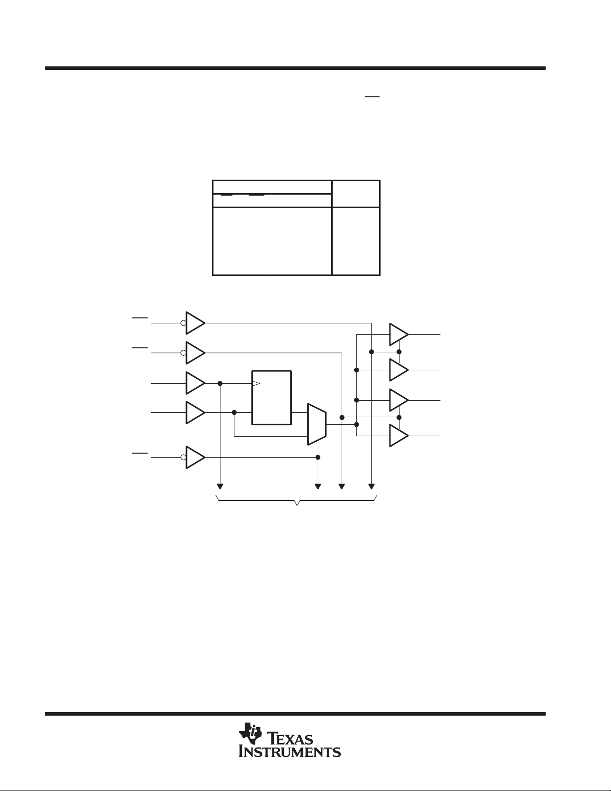
FUNCTION TABLE
INPUTS
OE SEL CLK A
H X X X Z
L HXL L
LHXH H
LL↑LL
LL↑HH
logic diagram (positive logic)
OUTPUT
Y
OE1
OE2
CLK
A1
SEL
20
21
19
8
22
CLK
D Q
To Eight Other Channels
5
1Y1
4
2Y1
2
3Y1
1
4Y1
2
POST OFFICE BOX 655303 • DALLAS, TEXAS 75265
IOHHigh-level output current
mA
IOLLow-level output current
mA
SN74ALVCH16831
1-TO-4 ADDRESS REGISTER/DRIVER
WITH 3-STATE OUTPUTS
SCES083D – AUGUST 1996 – REVISED FEBRUARY 1999
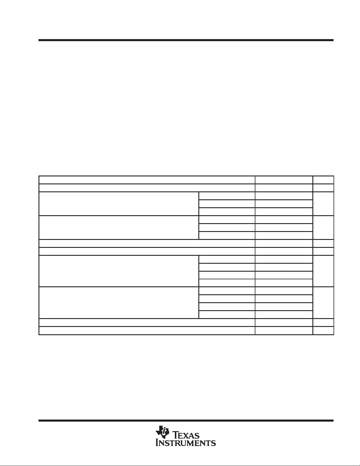
absolute maximum ratings over operating free-air temperature range (unless otherwise noted)
Supply voltage range, V
Input voltage range, V
Output voltage range, V
Input clamp current, I
Output clamp current, I
Continuous output current, I
Continuous current through each V
Package thermal impedance, θ
Storage temperature range, T
†
Stresses beyond those listed under “absolute maximum ratings” may cause permanent damage to the device. These are stress ratings only, and
functional operation of the device at these or any other conditions beyond those indicated under “recommended operating conditions” is not
implied. Exposure to absolute-maximum-rated conditions for extended periods may affect device reliability.
NOTES: 1. The input negative-voltage and output voltage ratings may be exceeded if the input and output current ratings are observed.
2. This value is limited to 4.6 V maximum.
3. The package thermal impedance is calculated in accordance with JESD 51.
–0.5 V to 4.6 V. . . . . . . . . . . . . . . . . . . . . . . . . . . . . . . . . . . . . . . . . . . . . . . . . . . . . . . . .
CC
(see Note 1) –0.5 V to 4.6 V. . . . . . . . . . . . . . . . . . . . . . . . . . . . . . . . . . . . . . . . . . . . . . . . .
I
(see Notes 1 and 2) –0.5 V to VCC + 0.5 V. . . . . . . . . . . . . . . . . . . . . . . . . . . . . . . . . .
O
(VI < 0) –50 mA. . . . . . . . . . . . . . . . . . . . . . . . . . . . . . . . . . . . . . . . . . . . . . . . . . . . . . . . . . .
IK
(VO < 0) –50 mA. . . . . . . . . . . . . . . . . . . . . . . . . . . . . . . . . . . . . . . . . . . . . . . . . . . . . . . .
OK
±50 mA. . . . . . . . . . . . . . . . . . . . . . . . . . . . . . . . . . . . . . . . . . . . . . . . . . . . . . . . . . . . .
O
JA
stg
or GND ±100 mA. . . . . . . . . . . . . . . . . . . . . . . . . . . . . . . . . . . . . . . . . . . . .
CC
(see Note 3) 106°C/W. . . . . . . . . . . . . . . . . . . . . . . . . . . . . . . . . . . . . . . . . . . . .
–65°C to 150°C. . . . . . . . . . . . . . . . . . . . . . . . . . . . . . . . . . . . . . . . . . . . . . . . . . .
†
recommended operating conditions (see Note 4)
MIN MAX UNIT
V
V
V
V
V
∆t/∆v Input transition rise or fall rate 10 ns/V
T
NOTE 4: All unused control inputs of the device must be held at VCC or GND to ensure proper device operation. Refer to the TI application report,
Supply voltage 1.65 3.6 V
CC
VCC = 1.65 V to 1.95 V 0.65 × V
High-level input voltage
IH
Low-level input voltage
IL
Input voltage 0 V
I
Output voltage 0 V
O
p
p
Operating free-air temperature –40 85 °C
A
Implications of Slow or Floating CMOS Inputs
, literature number SCBA004.
VCC = 2.3 V to 2.7 V
VCC = 2.7 V to 3.6 V 2
VCC = 1.65 V to 1.95 V 0.35 × V
VCC = 2.3 V to 2.7 V
VCC = 2.7 V to 3.6 V 0.8
VCC = 1.65 V –4
VCC = 2.3 V –12
VCC = 2.7 V –12
VCC = 3 V –24
VCC = 1.65 V 4
VCC = 2.3 V 12
VCC = 2.7 V 12
VCC = 3 V 24
CC
1.7
0.7
CC
CC
V
CC
V
V
V
POST OFFICE BOX 655303 • DALLAS, TEXAS 75265
3
 Loading...