

Texas Instruments SN74ALVCH16282DBBR Datasheet
SN74ALVCH16282
18-BIT TO 36-BIT REGISTERED BUS EXCHANGER
WITH 3-STATE OUTPUTS
SCES036D – JULY 1995 – REVISED MARCH 2000
1
POST OFFICE BOX 655303 • DALLAS, TEXAS 75265
D
Member of the Texas Instruments
Widebus
Family
D
EPIC
(Enhanced-Performance Implanted
CMOS) Submicron Process
D
ESD Protection Exceeds 2000 V Per
MIL-STD-883, Method 3015; Exceeds 200 V
Using Machine Model (C = 200 pF, R = 0)
D
Latch-up Performance Exceeds 250 mA Per
JESD 17
D
Bus Hold on Data Inputs Eliminates the
Need for External Pullup/Pulldown
Resistors
D
Packaged in Thin Very Small-Outline
Package
NOTE: For tape and reel order entry:
The DBBR package is abbreviated to GR.
description
The SN74ALVCH16282 is an 18-bit to 36-bit
registered bus exchanger designed for 1.65-V to
3.6-V VCC operation.
This device is intended for use in applications in
which data must be transferred from a narrow
high-speed bus to a wide lower-frequency bus. It
is designed specifically for low-voltage (3.3-V)
V
CC
operation.
The device provides synchronous data exchange
between the two ports. Data is stored in the
internal registers on the low-to-high transition of
the clock (CLK) input. For data transfer in the
B-to-A direction, the select (SEL) input selects 1B
or 2B data for the A outputs.
For data transfer in the A-to-B direction, a
two-stage pipeline is provided in the 1B path, with
a single storage register in the 2B path. Data flow
is controlled by the active-low output enable (OE
)
and the DIR input. The DIR control pin is
registered to synchronize the bus direction
changes with the clock.
Active bus-hold circuitry is provided to hold
unused or floating data inputs at a valid logic level.
The SN74ALVCH16282 is characterized for
operation from –40°C to 85°C.
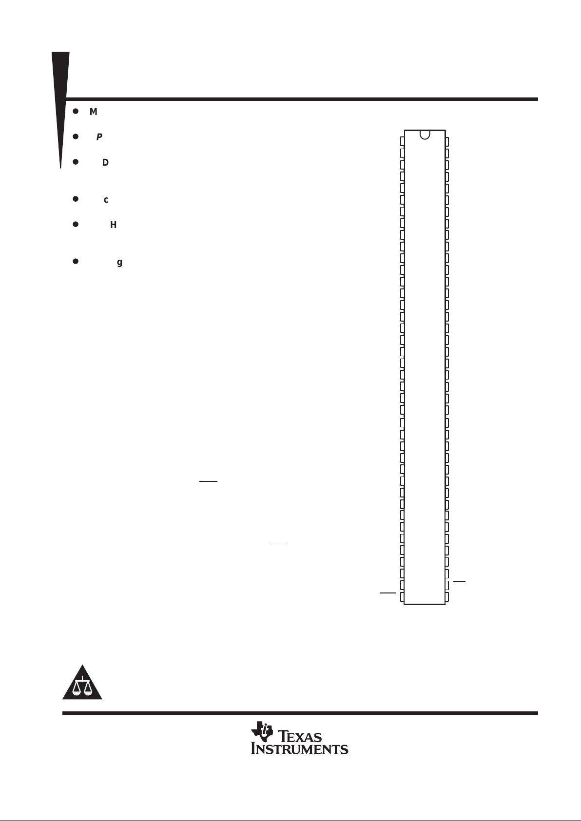
1
2
3
4
5
6
7
8
9
10
11
12
13
14
15
16
17
18
19
20
21
22
23
24
25
26
27
28
29
30
31
32
33
34
35
36
37
38
39
40
80
79
78
77
76
75
74
73
72
71
70
69
68
67
66
65
64
63
62
61
60
59
58
57
56
55
54
53
52
51
50
49
48
47
46
45
44
43
42
41
V
CC
GND
2B9
1B9
2B8
GND
1B8
2B7
1B7
V
CC
2B6
1B6
2B5
1B5
GND
2B4
1B4
2B3
1B3
V
CC
GND
2B2
1B2
2B1
1B1
V
CC
A1
A2
A3
GND
A4
A5
A6
V
CC
A7
A8
A9
GND
CLK
SEL
V
CC
GND
1B10
2B10
1B11
GND
2B11
1B12
2B12
V
CC
1B13
2B13
1B14
2B14
GND
1B15
2B15
1B16
2B16
V
CC
GND
1B17
2B17
1B18
2B18
V
CC
A18
A17
A16
GND
A15
A14
A13
V
CC
A12
A11
A10
GND
OE
DIR
DBB PACKAGE
(TOP VIEW)
Copyright 2000, Texas Instruments Incorporated
Please be aware that an important notice concerning availability, standard warranty, and use in critical applications of
Texas Instruments semiconductor products and disclaimers thereto appears at the end of this data sheet.
EPIC and Widebus are trademarks of Texas Instruments.
PRODUCTION DATA information is current as of publication date.
Products conform to specifications per the terms of Texas Instruments
standard warranty. Production processing does not necessarily include
testing of all parameters.
SN74ALVCH16282
18-BIT TO 36-BIT REGISTERED BUS EXCHANGER
WITH 3-STATE OUTPUTS
SCES036D – JULY 1995 – REVISED MARCH 2000
2
POST OFFICE BOX 655303 • DALLAS, TEXAS 75265
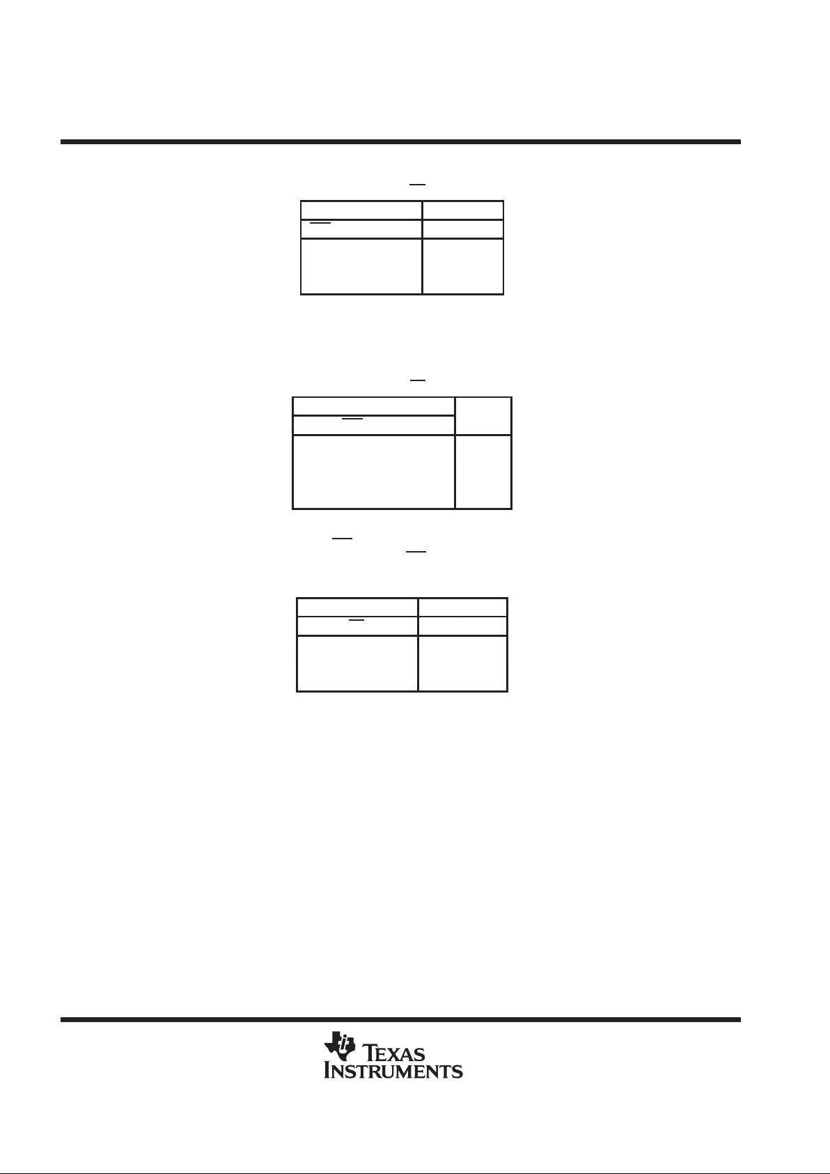
Function Tables
A-TO-B STORAGE (OE = L, DIR = H)
INPUTS
OUTPUTS
SEL CLK A 1B 2B
H X X 1B
0
†
2B
0
†
L ↑ LL‡X
L ↑ H H
‡
X
†
Output level before indicated
steady-state input conditions were
established
‡
Two CLK edges are needed to propagate
the data.
B-TO-A STORAGE (OE
= L, DIR = L)
INPUTS
OUTPUT
CLK SEL 1B 2B
A
↑ H X L L
§
↑ HXH H
§
↑ LLX L
↑ L H X H
§
Two CLK edges are needed to propagate the
data. The data is loaded in the first register
when SEL
is low and propagates to the
second register when SEL
is high.
OUTPUT ENABLE
INPUTS
OUTPUTS
CLK OE DIR A 1B, 2B
↑ H X Z Z
↑ LHZActive
↑ L L Active Z
SN74ALVCH16282
18-BIT TO 36-BIT REGISTERED BUS EXCHANGER
WITH 3-STATE OUTPUTS
SCES036D – JULY 1995 – REVISED MARCH 2000
3
POST OFFICE BOX 655303 • DALLAS, TEXAS 75265
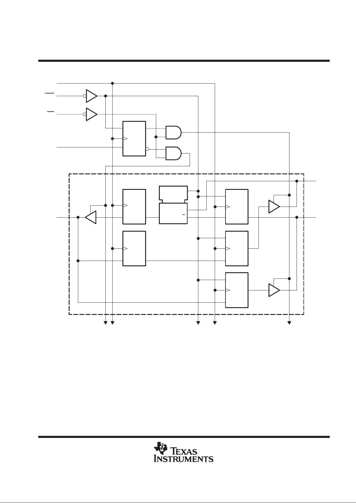
logic diagram (positive logic)
C1
1D
C1
G1
1
1
C1
CE
1D
C1
CE
C1
CE
1D
1D
C1
CE
1D
1 of 18 Channels
39
40
42
41
27
25
24
CLK
SEL
OE
DIR
A1
1B1
2B1
1D
 Loading...