

Texas Instruments SN74ALVCH162525DGGR, SN74ALVCH162525DL, SN74ALVCH162525DLR, SN74ALVCH162525GR Datasheet
SN74ALVCH162525
18-BIT REGISTERED BUS TRANSCEIVER
WITH 3-STATE OUTPUTS
SCES058F – NOVEMBER 1995 – REVISED SEPTEMBER 1999
1
POST OFFICE BOX 655303 • DALLAS, TEXAS 75265
D
Member of the Texas Instruments
Widebus
Family
D
EPIC
(Enhanced-Performance Implanted
CMOS) Submicron Process
D
B-Port Outputs Have Equivalent 26-Ω
Series Resistors, So No External Resistors
Are Required
D
ESD Protection Exceeds 2000 V Per
MIL-STD-883, Method 3015; Exceeds 200 V
Using Machine Model (C = 200 pF, R = 0)
D
Latch-Up Performance Exceeds 250 mA Per
JESD 17
D
Bus Hold on Data Inputs Eliminates the
Need for External Pullup/Pulldown
Resistors
D
Package Option Includes Plastic 300-mil
Shrink Small-Outline (DL) and Thin Shrink
Small-Outline (DGG) Packages
NOTE: For tape and reel order entry:
The DGGR package is abbreviated to GR.
description
This 18-bit universal bus transceiver is designed
for 1.65-V to 3.6-V V
CC
operation.
Data flow in each direction is controlled by
output-enable (OEAB
and OEBA) and
clock-enable (CLKENAB
and CLKENBA) inputs.
For the A-to-B data flow, the data flows through a
single register. The B-to-A data can flow through
a four-stage pipeline register path, or through a
single register path, depending on the state of the
select (SEL
) input.
Data is stored in the internal registers on the low-to-high transition of the clock (CLK) input, provided that the
appropriate CLKEN inputs are low. The A-to-B data transfer is synchronized to the CLKAB input, and B-to-A
data transfer is synchronized with the CLK1BA and CLK2BA inputs.
The B outputs, which are designed to sink up to 12 mA, include equivalent 26-Ω resistors to reduce overshoot
and undershoot.
T o ensure the high-impedance state during power up or power down, OE should be tied to VCC through a pullup
resistor; the minimum value of the resistor is determined by the current-sinking capability of the driver.
Active bus-hold circuitry is provided to hold unused or floating data inputs at a valid logic level.
The SN74ALVCH162525 is characterized for operation from –40°C to 85°C.
Copyright 1999, Texas Instruments Incorporated
PRODUCTION DATA information is current as of publication date.
Products conform to specifications per the terms of Texas Instruments
standard warranty. Production processing does not necessarily include
testing of all parameters.
EPIC and Widebus are trademarks of Texas Instruments Incorporated.
Please be aware that an important notice concerning availability, standard warranty, and use in critical applications of
Texas Instruments semiconductor products and disclaimers thereto appears at the end of this data sheet.
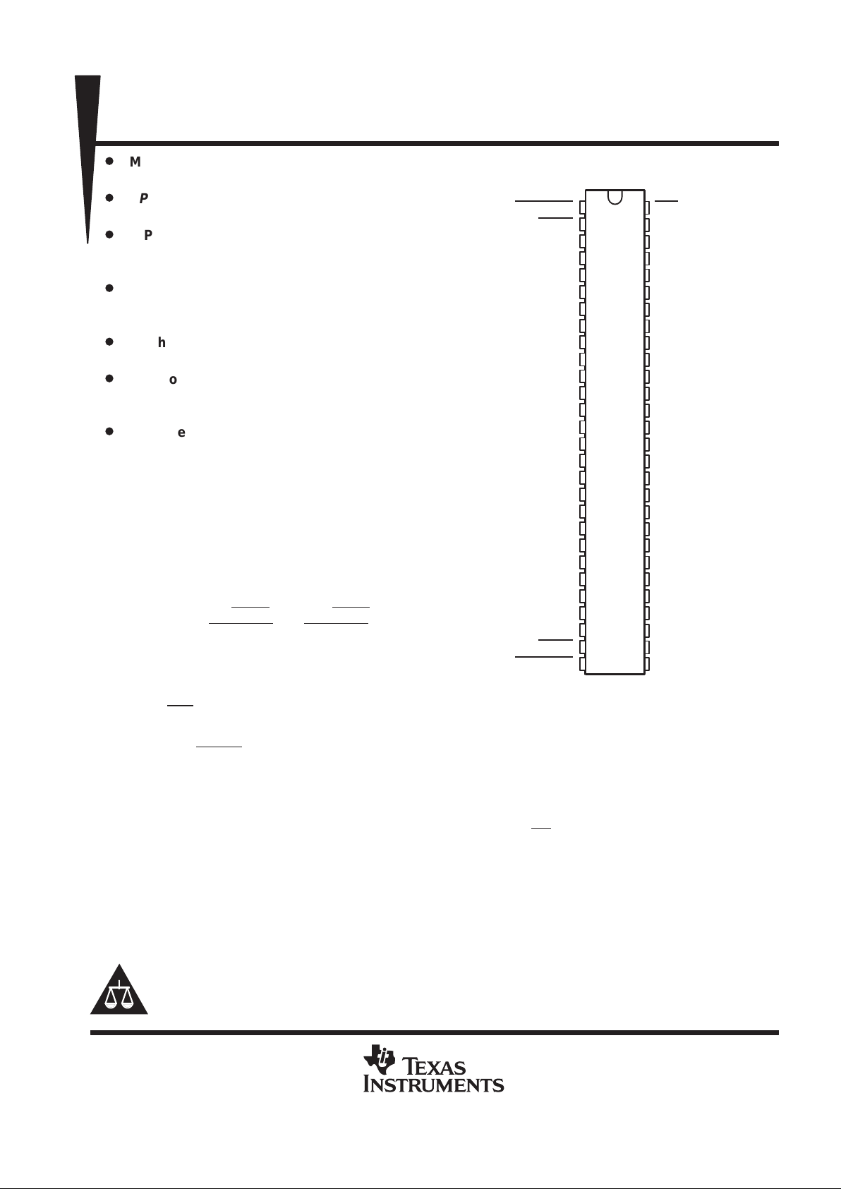
DGG OR DL PACKAGE
(TOP VIEW)
1
2
3
4
5
6
7
8
9
10
11
12
13
14
15
16
17
18
19
20
21
22
23
24
25
26
27
28
56
55
54
53
52
51
50
49
48
47
46
45
44
43
42
41
40
39
38
37
36
35
34
33
32
31
30
29
CLKENAB
OEAB
A1
GND
A2
A3
V
CC
A4
A5
A6
GND
A7
A8
A9
A10
A11
A12
GND
A13
A14
A15
V
CC
A16
A17
GND
A18
OEBA
CLKENBA
SEL
CLKAB
B1
GND
B2
B3
V
CC
B4
B5
B6
GND
B7
B8
B9
B10
B11
B12
GND
B13
B14
B15
V
CC
B16
B17
GND
B18
CLK1BA
CLK2BA
SN74ALVCH162525
18-BIT REGISTERED BUS TRANSCEIVER
WITH 3-STATE OUTPUTS
SCES058F – NOVEMBER 1995 – REVISED SEPTEMBER 1999
2
POST OFFICE BOX 655303 • DALLAS, TEXAS 75265
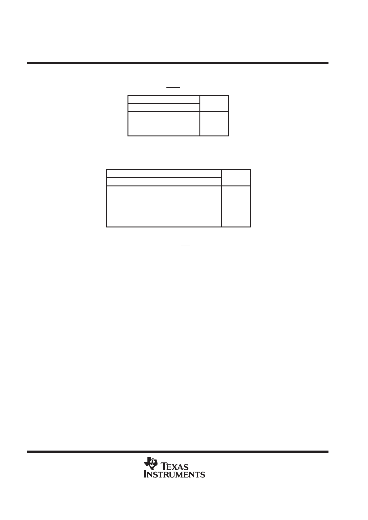
Function Tables
A-TO-B STORAGE
(OEAB
= L)
INPUTS
OUTPUT
CLKENAB CLKAB A
B
H X X B
0
†
L ↑ LL
L ↑ H H
†
Output level before the indicated steady-state
input conditions were established
B-TO-A STORAGE
(OEBA
= L)
INPUTS
OUTPUT
CLKENBA CLK2BA CLK1BA SEL B
A
H X X X X A
0
†
L ↑ XHL L
L ↑ XHHH
L ↑↑LL L
‡
L ↑ ↑ L H H
‡
†
Output level before the indicated steady-state input conditions were
established
‡
Three CLK1BA edges and one CLK2BA edge are needed to
propagate data from B to A when SEL
is low.
SN74ALVCH162525
18-BIT REGISTERED BUS TRANSCEIVER
WITH 3-STATE OUTPUTS
SCES058F – NOVEMBER 1995 – REVISED SEPTEMBER 1999
3
POST OFFICE BOX 655303 • DALLAS, TEXAS 75265
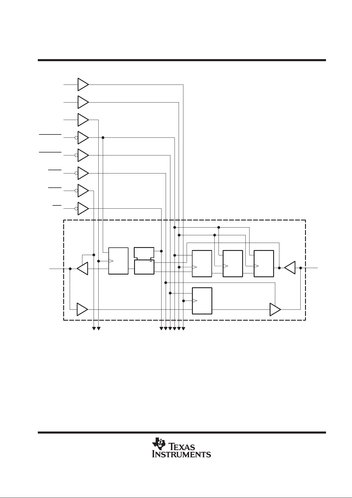
logic diagram (positive logic)
B1
CLKAB
CLK1BA
CLK2BA
CLKENBA
CLKENAB
OEAB
OEBA
SEL
CE
C1
1D
A1
CE
C1
1D
CE
C1
1D
CE
C1
1D
CE
C1
1D
1
1
1 of 18 Channels
G1
55
30
29
28
1
2
27
56
3
54

SN74ALVCH162525
18-BIT REGISTERED BUS TRANSCEIVER
WITH 3-STATE OUTPUTS
SCES058F – NOVEMBER 1995 – REVISED SEPTEMBER 1999
4
POST OFFICE BOX 655303 • DALLAS, TEXAS 75265
absolute maximum ratings over operating free-air temperature range (unless otherwise noted)
†
Supply voltage range, VCC –0.5 V to 4.6 V. . . . . . . . . . . . . . . . . . . . . . . . . . . . . . . . . . . . . . . . . . . . . . . . . . . . . . . . .
Input voltage range, VI: Except I/O ports (see Note 1) –0.5 V to 4.6 V. . . . . . . . . . . . . . . . . . . . . . . . . . . . . . . . .
I/O ports (see Notes 1 and 2) –0.5 V to V
CC
+ 0.5 V. . . . . . . . . . . . . . . . . . . . . . . . . . .
Output voltage range, VO (see Notes 1 and 2) –0.5 V to VCC + 0.5 V. . . . . . . . . . . . . . . . . . . . . . . . . . . . . . . . . .
Input clamp current, IIK (VI < 0) –50 mA. . . . . . . . . . . . . . . . . . . . . . . . . . . . . . . . . . . . . . . . . . . . . . . . . . . . . . . . . . .
Output clamp current, IOK (VO < 0) –50 mA. . . . . . . . . . . . . . . . . . . . . . . . . . . . . . . . . . . . . . . . . . . . . . . . . . . . . . . .
Continuous output current, IO ±50 mA. . . . . . . . . . . . . . . . . . . . . . . . . . . . . . . . . . . . . . . . . . . . . . . . . . . . . . . . . . . . .
Continuous current through each V
CC
or GND ±100 mA. . . . . . . . . . . . . . . . . . . . . . . . . . . . . . . . . . . . . . . . . . . . .
Package thermal impedance, θJA (see Note 3): DGG package 81°C/W. . . . . . . . . . . . . . . . . . . . . . . . . . . . . . .
DL package 74°C/W. . . . . . . . . . . . . . . . . . . . . . . . . . . . . . . . .
Storage temperature range, T
stg
–65°C to 150°C. . . . . . . . . . . . . . . . . . . . . . . . . . . . . . . . . . . . . . . . . . . . . . . . . . .
†
Stresses beyond those listed under “absolute maximum ratings” may cause permanent damage to the device. These are stress ratings only, and
functional operation of the device at these or any other conditions beyond those indicated under “recommended operating conditions” is not
implied. Exposure to absolute-maximum-rated conditions for extended periods may affect device reliability.
NOTES: 1. The input negative-voltage and output voltage ratings may be exceeded if the input and output current ratings are observed.
2. This value is limited to 4.6 V maximum.
3. The package thermal impedance is calculated in accordance with JESD 51.

SN74ALVCH162525
18-BIT REGISTERED BUS TRANSCEIVER
WITH 3-STATE OUTPUTS
SCES058F – NOVEMBER 1995 – REVISED SEPTEMBER 1999
5
POST OFFICE BOX 655303 • DALLAS, TEXAS 75265
recommended operating conditions (see Note 4)
MIN MAX UNIT
V
CC
Supply voltage 1.65 3.6 V
VCC = 1.65 V to 1.95 V 0.65 × V
CC
V
IH
High-level input voltage
VCC = 2.3 V to 2.7 V
1.7
V
VCC = 2.7 V to 3.6 V 2
VCC = 1.65 V to 1.95 V 0.35 × V
CC
V
IL
Low-level input voltage
VCC = 2.3 V to 2.7 V
0.7
V
VCC = 2.7 V to 3.6 V 0.8
V
I
Input voltage 0 V
CC
V
V
O
Output voltage 0 V
CC
V
VCC = 1.65 V –4
p
p
VCC = 2.3 V –12
High-level output current (A port)
VCC = 2.7 V –12
VCC = 3 V –24
I
OH
VCC = 1.65 V –2
mA
p
p
VCC = 2.3 V –6
High-level output current (B port)
VCC = 2.7 V –8
VCC = 3 V –12
VCC = 1.65 V 4
p
p
VCC = 2.3 V 12
Low-level output current (A port)
VCC = 2.7 V 12
VCC = 3 V 24
I
OL
VCC = 1.65 V 2
mA
p
p
VCC = 2.3 V 6
Low-level output current (B port)
VCC = 2.7 V 8
VCC = 3 V 12
∆t/∆v Input transition rise or fall rate 10 ns/V
T
A
Operating free-air temperature –40 85 °C
NOTE 4: All unused control inputs of the device must be held at VCC or GND to ensure proper device operation. Refer to the TI application report,
Implications of Slow or Floating CMOS Inputs
, literature number SCBA004.

SN74ALVCH162525
18-BIT REGISTERED BUS TRANSCEIVER
WITH 3-STATE OUTPUTS
SCES058F – NOVEMBER 1995 – REVISED SEPTEMBER 1999
6
POST OFFICE BOX 655303 • DALLAS, TEXAS 75265
electrical characteristics over recommended operating free-air temperature range (unless
otherwise noted)
PARAMETER TEST CONDITIONS
V
CC
MIN TYP†MAX UNIT
IOH = –100 µA 1.65 V to 3.6 V VCC–0.2
IOH = –4 mA 1.65 V 1.2
IOH = –6 mA 2.3 V 2
A port
2.3 V 1.7
IOH = –12 mA
2.7 V 2.2
3 V 2.4
IOH = –24 mA 3 V 2
V
OH
IOH = –100 µA 1.65 V to 3.6 V VCC–0.2
V
IOH = –2 mA 1.65 V 1.2
IOH = –4 mA 2.3 V 1.9
B port
2.3 V 1.7
I
OH
= –6
mA
3 V 2.4
IOH = –8 mA 2.7 V 2
IOH = –12 mA 3 V 2
IOL = 100 µA 1.65 V to 3.6 V 0.2
IOL = 4 mA 1.65 V 0.45
p
IOL = 6 mA 2.3 V 0.4
A port
2.3 V 0.7
I
OL
= 12
mA
2.7 V 0.4
IOL = 24 mA 3 V 0.55
V
OL
IOL = 100 µA 1.65 V to 3.6 V 0.2
V
IOL = 2 mA 1.65 V 0.45
IOL = 4 mA 2.3 V 0.4
B port
2.3 V 0.55
I
OL
= 6
mA
3 V 0.55
IOL = 8 mA 2.7 V 0.6
IOL = 12 mA 3 V 0.8
I
I
VI = VCC or GND 3.6 V ±5 µA
VI = 0.58 V
25
VI = 1.07 V
1.65 V
–25
VI = 0.7 V
45
I
I(hold)
VI = 1.7 V
2.3 V
–45
µA
()
VI = 0.8 V
75
VI = 2 V
3 V
–75
VI = 0 to 3.6 V
‡
3.6 V ±500
I
OZ
§
VO = VCC or GND 3.6 V ±10 µA
I
CC
VI = VCC or GND, IO = 0 3.6 V 40 µA
∆I
CC
One input at VCC – 0.6 V, Other inputs at VCC or GND 3 V to 3.6 V 750 µA
C
i
Control inputs VI = VCC or GND 3.3 V 3 pF
C
io
A or B ports VO = VCC or GND 3.3 V 7 pF
†
All typical values are at VCC = 3.3 V, TA = 25°C.
‡
This is the bus-hold maximum dynamic current. It is the minimum overdrive current required to switch the input from one state to another.
§
For I/O ports, the parameter IOZ includes the input leakage current.

SN74ALVCH162525
18-BIT REGISTERED BUS TRANSCEIVER
WITH 3-STATE OUTPUTS
SCES058F – NOVEMBER 1995 – REVISED SEPTEMBER 1999
7
POST OFFICE BOX 655303 • DALLAS, TEXAS 75265
timing requirements over recommended operating free-air temperature range (unless otherwise
noted) (see Figures 1 through 3)
VCC = 1.8 V
VCC = 2.5 V
± 0.2 V
VCC = 2.7 V
VCC = 3.3 V
± 0.3 V
UNIT
MIN MAX MIN MAX MIN MAX MIN MAX
f
clock
Clock frequency
†
120 125 150 MHz
t
w
Pulse duration, CLK high or low
†
3.2 3.2 3 ns
A data before CLKAB↑
†
1.3 1.3 1.3
B data before CLK2BA↑
†
2.1 1.8 1.7
B data before CLK1BA↑
†
1.3 1.2 1.1
t
su
Setup time
SEL
before CLK2BA↑
†
3.3 3.3 3.3
ns
CLKENAB before CLKAB↑
†
2.1 1.9 1.6
CLKENBA before CLK1BA↑
†
2.7 2.5 2.1
CLKENBA before CLK2BA↑
†
2.7 2.5 2.2
A data after CLKAB↑
†
0.7 0.4 0.9
B data after CLK2BA↑
†
0.4 0 0.6
B data after CLK1BA↑
†
0.8 0.4 1
t
h
Hold time
SEL
after CLK2BA↑
†
0 0 0.1
ns
CLKENAB after CLKAB↑
†
0.1 0.3 0.3
CLKENBA after CLK1BA↑
†
0 0 0.1
CLKENBA after CLK2BA↑
†
0 0 0
†
This information was not available at the time of publication.
switching characteristics over recommended operating free-air temperature range (unless
otherwise noted) (see Figures 1 through 3)
PARAMETER
FROM
TO
VCC = 1.8 V
VCC = 2.5 V
± 0.2 V
VCC = 2.7 V
VCC = 3.3 V
± 0.3 V
UNIT
(INPUT)
(OUTPUT)
MIN MAX MIN MAX MIN MAX MIN MAX
f
max
†
120 125 150 MHz
CLKAB B
†
1 5.5 5.4 1 4.7
t
pd
CLK2BA A
†
1 4.5 4.4 1 4.2
ns
OEBA A
†
1 6.1 6.1 1 5.1
t
en
OEAB
B
†
1 6.7 6.8 1 5.7
ns
OEBA A
†
1 6.3 5.4 1 4.9
t
dis
OEAB
B
†
1 6.3 5.4 1 4.9
ns
†
This information was not available at the time of publication.
operating characteristics, T
A
= 25°C
VCC = 1.8 V VCC = 2.5 V VCC = 3.3 V
PARAMETER
TEST CONDITIONS
TYP TYP TYP
UNIT
Power dissipation
Outputs enabled
p
†
160 160
p
C
pd
capacitance
Outputs disabled
C
L
=
50 pF
,f = 10 MHz
†
160 160
pF
†
This information was not available at the time of publication.
SN74ALVCH162525
18-BIT REGISTERED BUS TRANSCEIVER
WITH 3-STATE OUTPUTS
SCES058F – NOVEMBER 1995 – REVISED SEPTEMBER 1999
8
POST OFFICE BOX 655303 • DALLAS, TEXAS 75265
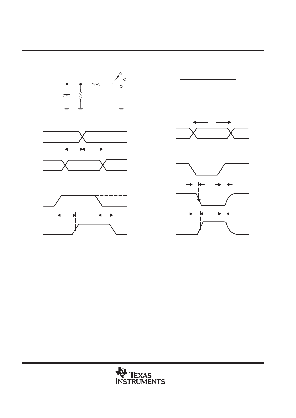
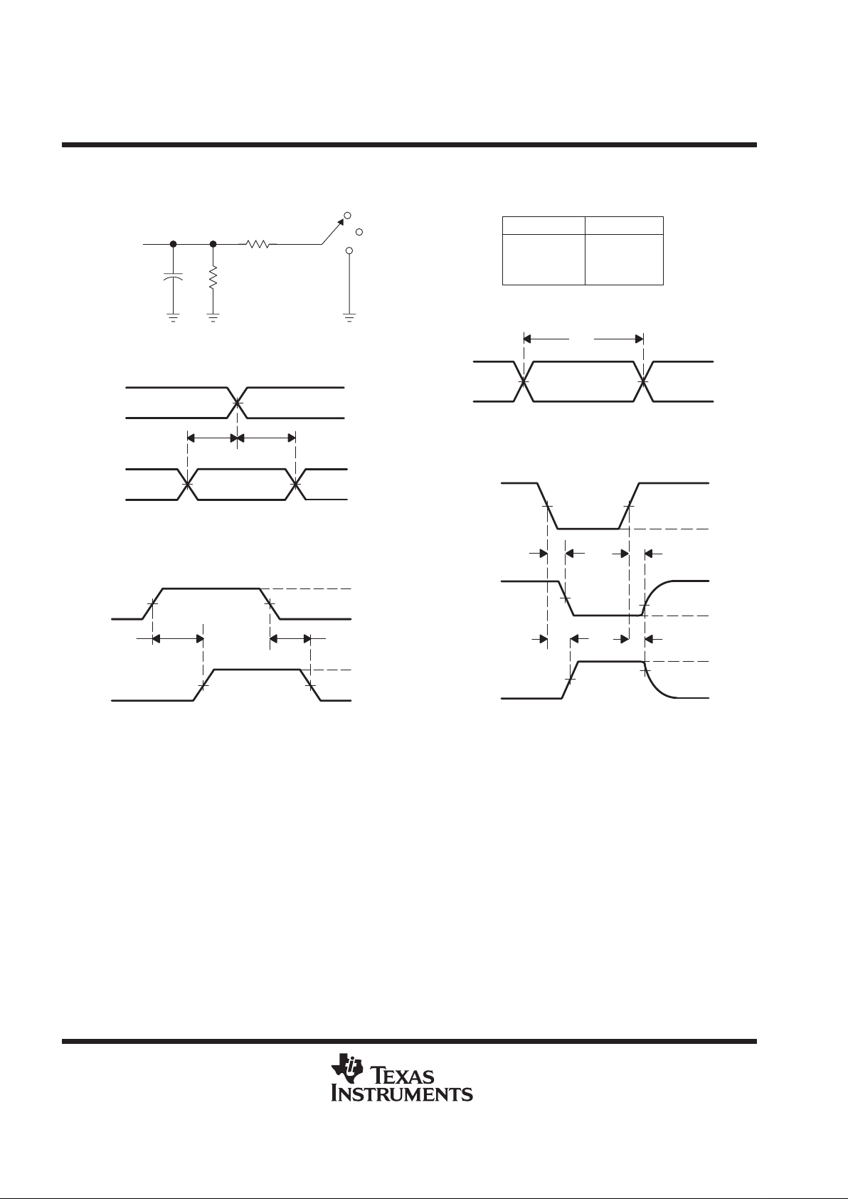
PARAMETER MEASUREMENT INFORMATION
V
CC
= 1.8 V
VCC/2
VCC/2
VCC/2VCC/2
VCC/2VCC/2
VCC/2
VCC/2
V
OH
V
OL
t
h
t
su
From Output
Under Test
CL = 30 pF
(see Note A)
LOAD CIRCUIT
S1
Open
GND
1 kΩ
1 kΩ
Output
Control
(low-level
enabling)
Output
Waveform 1
S1 at 2 × V
CC
(see Note B)
Output
Waveform 2
S1 at GND
(see Note B)
t
PZL
t
PZH
t
PLZ
t
PHZ
0 V
VOL + 0.15 V
VOH – 0.15 V
0 V
V
CC
0 V
0 V
t
w
V
CC
V
CC
VOLTAGE WAVEFORMS
SETUP AND HOLD TIMES
VOLTAGE WAVEFORMS
PULSE DURATION
VOLTAGE WAVEFORMS
ENABLE AND DISABLE TIMES
Timing
Input
Data
Input
Input
t
pd
t
PLZ/tPZL
t
PHZ/tPZH
Open
2 × V
CC
GND
TEST S1
NOTES: A. CL includes probe and jig capacitance.
B. Waveform 1 is for an output with internal conditions such that the output is low except when disabled by the output control.
Waveform 2 is for an output with internal conditions such that the output is high except when disabled by the output control.
C. All input pulses are supplied by generators having the following characteristics: PRR ≤ 10 MHz, ZO = 50 Ω, tr ≤ 2 ns, tf ≤ 2 ns.
D. The outputs are measured one at a time with one transition per measurement.
E. t
PLZ
and t
PHZ
are the same as t
dis
.
F. t
PZL
and t
PZH
are the same as ten.
G. t
PLH
and t
PHL
are the same as tpd.
0 V
V
CC
VCC/2
t
PHL
VCC/2 VCC/2
V
CC
0 V
V
OH
V
OL
Input
Output
VOLTAGE WAVEFORMS
PROPAGATION DELAY TIMES
VCC/2 VCC/2
t
PLH
2 × V
CC
V
CC
Figure 1. Load Circuit and Voltage Waveforms

SN74ALVCH162525
18-BIT REGISTERED BUS TRANSCEIVER
WITH 3-STATE OUTPUTS
SCES058F – NOVEMBER 1995 – REVISED SEPTEMBER 1999
9
POST OFFICE BOX 655303 • DALLAS, TEXAS 75265
PARAMETER MEASUREMENT INFORMATION
V
CC
= 2.5 V ± 0.2 V
VCC/2
VCC/2
VCC/2VCC/2
VCC/2VCC/2
VCC/2
VCC/2
V
OH
V
OL
t
h
t
su
From Output
Under Test
CL = 30 pF
(see Note A)
LOAD CIRCUIT
S1
Open
GND
500 Ω
500 Ω
Output
Control
(low-level
enabling)
Output
Waveform 1
S1 at 2 × V
CC
(see Note B)
Output
Waveform 2
S1 at GND
(see Note B)
t
PZL
t
PZH
t
PLZ
t
PHZ
0 V
VOL + 0.15 V
VOH – 0.15 V
0 V
V
CC
0 V
0 V
t
w
V
CC
V
CC
VOLTAGE WAVEFORMS
SETUP AND HOLD TIMES
VOLTAGE WAVEFORMS
PULSE DURATION
VOLTAGE WAVEFORMS
ENABLE AND DISABLE TIMES
Timing
Input
Data
Input
Input
t
pd
t
PLZ/tPZL
t
PHZ/tPZH
Open
2 × V
CC
GND
TEST S1
NOTES: A. CL includes probe and jig capacitance.
B. Waveform 1 is for an output with internal conditions such that the output is low except when disabled by the output control.
Waveform 2 is for an output with internal conditions such that the output is high except when disabled by the output control.
C. All input pulses are supplied by generators having the following characteristics: PRR ≤ 10 MHz, ZO = 50 Ω, tr ≤ 2 ns, tf ≤ 2 ns.
D. The outputs are measured one at a time with one transition per measurement.
E. t
PLZ
and t
PHZ
are the same as t
dis
.
F. t
PZL
and t
PZH
are the same as ten.
G. t
PLH
and t
PHL
are the same as tpd.
0 V
V
CC
VCC/2
t
PHL
VCC/2 VCC/2
V
CC
0 V
V
OH
V
OL
Input
Output
VOLTAGE WAVEFORMS
PROPAGATION DELAY TIMES
VCC/2 VCC/2
t
PLH
2 × V
CC
V
CC
Figure 2. Load Circuit and Voltage Waveforms
SN74ALVCH162525
18-BIT REGISTERED BUS TRANSCEIVER
WITH 3-STATE OUTPUTS
SCES058F – NOVEMBER 1995 – REVISED SEPTEMBER 1999
10
POST OFFICE BOX 655303 • DALLAS, TEXAS 75265
PARAMETER MEASUREMENT INFORMATION
V
CC
= 2.7 V AND 3.3 V ± 0.3 V
V
OH
V
OL
t
h
t
su
From Output
Under Test
CL = 50 pF
(see Note A)
LOAD CIRCUIT
S1
6 V
Open
GND
500 Ω
500 Ω
t
PLH
t
PHL
Output
Control
(low-level
enabling)
Output
Waveform 1
S1 at 6 V
(see Note B)
Output
Waveform 2
S1 at GND
(see Note B)
t
PZL
t
PZH
t
PLZ
t
PHZ
1.5 V1.5 V
1.5 V 1.5 V
2.7 V
0 V
1.5 V 1.5 V
V
OH
V
OL
0 V
1.5 V
VOL + 0.3 V
1.5 V
VOH – 0.3 V
0 V
1.5 V
2.7 V
0 V
1.5 V 1.5 V
0 V
2.7 V
0 V
1.5 V 1.5 V
t
w
Input
2.7 V
2.7 V
3 V
VOLTAGE WAVEFORMS
SETUP AND HOLD TIMES
VOLTAGE WAVEFORMS
PROPAGATION DELAY TIMES
VOLTAGE WAVEFORMS
PULSE DURATION
VOLTAGE WAVEFORMS
ENABLE AND DISABLE TIMES
Timing
Input
Data
Input
Output
Input
t
pd
t
PLZ/tPZL
t
PHZ/tPZH
Open
6 V
GND
TEST S1
NOTES: A. CL includes probe and jig capacitance.
B. Waveform 1 is for an output with internal conditions such that the output is low except when disabled by the output control.
Waveform 2 is for an output with internal conditions such that the output is high except when disabled by the output control.
C. All input pulses are supplied by generators having the following characteristics: PRR ≤10 MHz, ZO = 50 Ω, tr ≤2.5 ns, tf ≤2.5 ns.
D. The outputs are measured one at a time with one transition per measurement.
E. t
PLZ
and t
PHZ
are the same as t
dis
.
F. t
PZL
and t
PZH
are the same as ten.
G. t
PLH
and t
PHL
are the same as tpd.
Figure 3. Load Circuit and Voltage Waveforms

IMPORTANT NOTICE
T exas Instruments and its subsidiaries (TI) reserve the right to make changes to their products or to discontinue
any product or service without notice, and advise customers to obtain the latest version of relevant information
to verify, before placing orders, that information being relied on is current and complete. All products are sold
subject to the terms and conditions of sale supplied at the time of order acknowledgement, including those
pertaining to warranty, patent infringement, and limitation of liability.
TI warrants performance of its semiconductor products to the specifications applicable at the time of sale in
accordance with TI’s standard warranty. Testing and other quality control techniques are utilized to the extent
TI deems necessary to support this warranty. Specific testing of all parameters of each device is not necessarily
performed, except those mandated by government requirements.
CERT AIN APPLICATIONS USING SEMICONDUCTOR PRODUCTS MAY INVOLVE POTENTIAL RISKS OF
DEATH, PERSONAL INJURY, OR SEVERE PROPERTY OR ENVIRONMENTAL DAMAGE (“CRITICAL
APPLICATIONS”). TI SEMICONDUCTOR PRODUCTS ARE NOT DESIGNED, AUTHORIZED, OR
WARRANTED TO BE SUITABLE FOR USE IN LIFE-SUPPORT DEVICES OR SYSTEMS OR OTHER
CRITICAL APPLICATIONS. INCLUSION OF TI PRODUCTS IN SUCH APPLICA TIONS IS UNDERSTOOD T O
BE FULLY AT THE CUSTOMER’S RISK.
In order to minimize risks associated with the customer’s applications, adequate design and operating
safeguards must be provided by the customer to minimize inherent or procedural hazards.
TI assumes no liability for applications assistance or customer product design. TI does not warrant or represent
that any license, either express or implied, is granted under any patent right, copyright, mask work right, or other
intellectual property right of TI covering or relating to any combination, machine, or process in which such
semiconductor products or services might be or are used. TI’s publication of information regarding any third
party’s products or services does not constitute TI’s approval, warranty or endorsement thereof.
Copyright 1999, Texas Instruments Incorporated
 Loading...