Texas Instruments SN74ALS992DW, SN74ALS992DWR, SN74ALS992NT Datasheet

SN74ALS992
9-BIT D-TYPE TRANSPARENT READ-BACK LATCH
WITH 3-STATE OUTPUTS
SDAS028B – APRIL 1984 – REVISED JANUARY 1995
Copyright 1995, Texas Instruments Incorporated
1
POST OFFICE BOX 655303 • DALLAS, TEXAS 75265
• 3-State I/O-Type Read-Back Inputs
• Bus-Structured Pinout
• True Logic Outputs
• Designed With Nine Bits for Parity
Applications
• Package Options Include Plastic
Small-Outline (DW) Packages and Standard
Plastic (NT) 300-mil DIPs
description
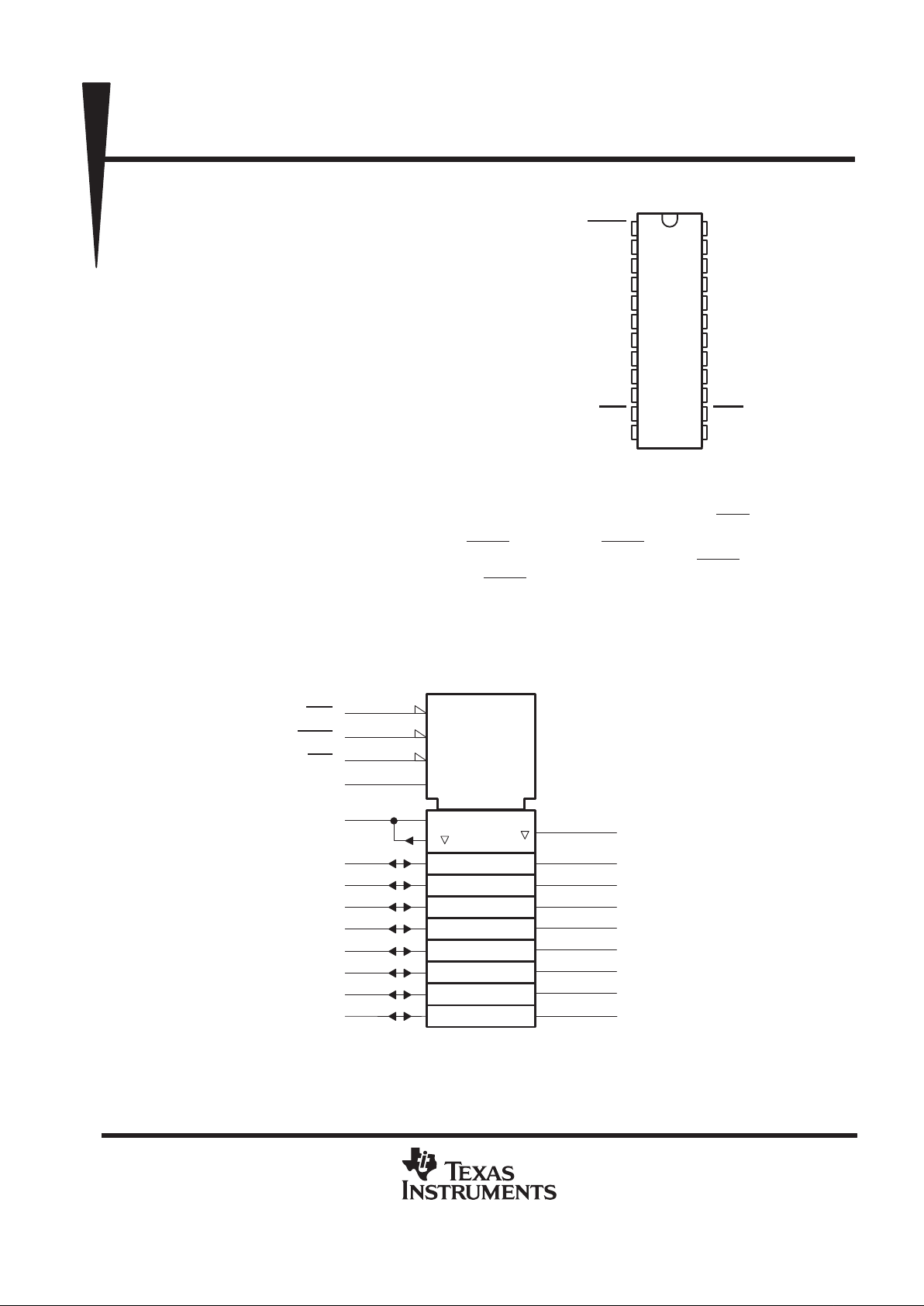
This 9-bit latch is designed specifically for storing
the contents of the input data bus and providing
the capability of reading back the stored data onto
the input data bus. In addition, this device provides
a 3-state buffer-type output and is easily
implemented in parity applications.
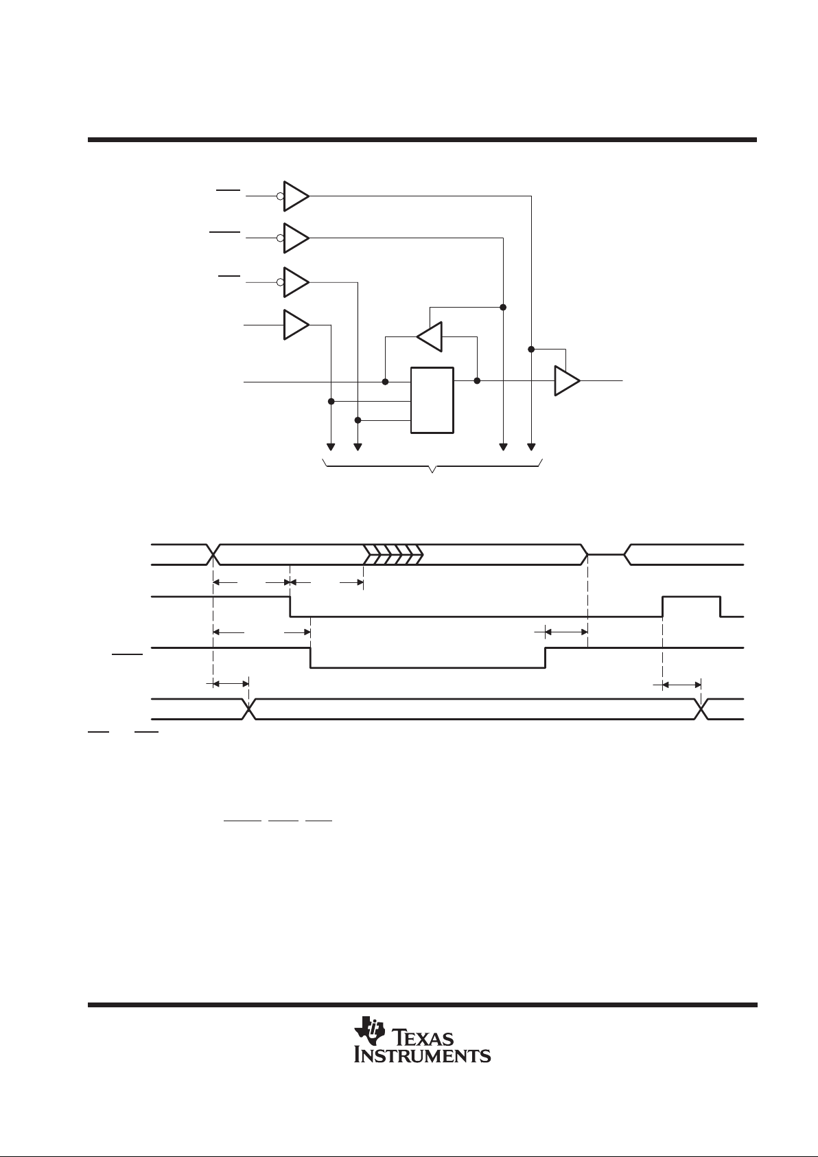
The nine latches are transparent D-type latches. While the latch-enable (LE) input is high, the Q outputs follow
the data (D) inputs. The Q outputs are in the 3-state condition when the output-enable (OEQ
) input is high.
Read back is provided through the output-enable (OERB
) input. When OERB is taken low, the data present at
the output of the data latches is allowed to pass back onto the input data bus. When OERB
is taken high, the
output of the data latches is isolated from the D inputs. OERB
does not affect the internal operation of the latches;
however, precautions should be taken not to create a bus conflict.
The SN74ALS992 is characterized for operation from 0°C to 70°C.
logic symbol
†
C1
13
LE
2D
3
3D
4
4D
5
5D
6
6D
7
7D
8
8D
9
2
5Q
19
6Q
18
7Q
17
8Q
16
2Q
22
3Q
21
4Q
20
1Q
23
1D
2
1D
R
11
CLR
EN2
1
OERB
EN3
14
OEQ
3
9D
10
9Q
15
†
This symbol is in accordance with ANSI/IEEE Std 91-1984 and IEC Publication 617-12.
DW OR NT PACKAGE
(TOP VIEW)
1
2
3
4
5
6
7
8
9
10
11
12
24
23
22
21
20
19
18
17
16
15
14
13
OERB
1D
2D
3D
4D
5D
6D
7D
8D
9D
CLR
GND
V
CC
1Q
2Q
3Q
4Q
5Q
6Q
7Q
8Q
9Q
OEQ
LE
PRODUCTION DATA information is current as of publication date.
Products conform to specifications per the terms of Texas Instruments
standard warranty. Production processing does not necessarily include
testing of all parameters.

SN74ALS992
9-BIT D-TYPE TRANSPARENT READ-BACK LATCH
WITH 3-STATE OUTPUTS
SDAS028B – APRIL 1984 – REVISED JANUARY 1995
2
POST OFFICE BOX 655303 • DALLAS, TEXAS 75265
logic diagram (positive logic)
1D
C1
To Eight Other Channels
1
13
2
23
OERB
LE
1D
1Q
14
OEQ
11
CLR
R
timing diagram
Data Bus
LE
OERB
Q
t
su
t
h
t
pd
t
dis
Input Data Read Back Input Data
t
pd
t
su
†
CLR
= H, OEQ = L
†
This setup time ensures that the read-back circuit will not create a conflict on the input data bus.
absolute maximum ratings over operating free-air temperature range (unless otherwise noted)
‡
Supply voltage, V
CC
7 V. . . . . . . . . . . . . . . . . . . . . . . . . . . . . . . . . . . . . . . . . . . . . . . . . . . . . . . . . . . . . . . . . . . . . . . .
Input voltage, V
I
(OERB, OEQ, CLR, and LE) 7 V. . . . . . . . . . . . . . . . . . . . . . . . . . . . . . . . . . . . . . . . . . . . . . . . . . .
Voltage applied to D inputs and to disabled 3-state outputs 5.5 V. . . . . . . . . . . . . . . . . . . . . . . . . . . . . . . . . . . . .
Operating free-air temperature range, T
A
0°C to 70°C. . . . . . . . . . . . . . . . . . . . . . . . . . . . . . . . . . . . . . . . . . . . . .
Storage temperature range –65°C to 150°C. . . . . . . . . . . . . . . . . . . . . . . . . . . . . . . . . . . . . . . . . . . . . . . . . . . . . . .
‡
Stresses beyond those listed under “absolute maximum ratings” may cause permanent damage to the device. These are stress ratings only, and
functional operation of the device at these or any other conditions beyond those indicated under “recommended operating conditions” is not
implied. Exposure to absolute-maximum-rated conditions for extended periods may affect device reliability.
 Loading...