

SN74ALS679
12-BIT ADDRESS COMPARATOR
SDAS003C – JUNE 1982 – REVISED JANUARY 1995
• 12-Bit Address Comparator With Enable
• Package Options Include Plastic
Small-Outline (DW) Packages and Standard
Plastic (N) 300-mil DIPs
description
This 12-bit address comparator simplifies
addressing of memory boards and/or other
peripheral devices. The four P inputs are normally
hardwired with a preprogrammed address. An
internal decoder determines what input
information applied to the A inputs must be low or
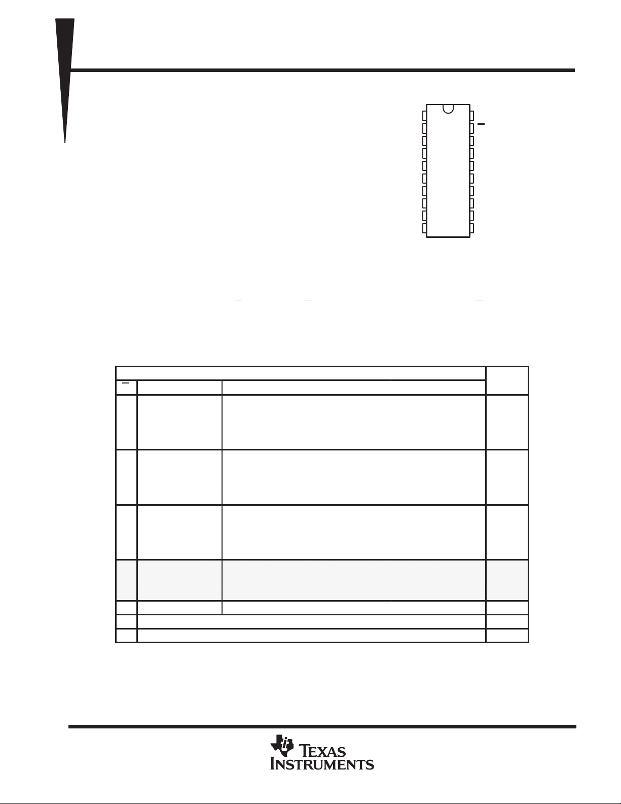
DW OR N PACKAGE
(TOP VIEW)
1
2
3
4
5
6
7
8
9
10
20
19
18
17
16
15
14
13
12
11
A1
A2
A3
A4
A5
A6
A7
A8
A9
GND
V
CC
G
Y
P3
P2
P1
P0
A12
A1 1
A10
high to cause a low state at the Y output. For
example, a positive-logic bit combination of 0111
(decimal 7) at the P input determines that inputs A1 through A7 must be low and that inputs A8 through A12 must
be high to cause the output to go low. Equality of the address applied at the A inputs to the preprogrammed
address is indicated by the output being low.
This device features an enable (G
) input. When G is low, the device is enabled. When G is high, the device is
disabled and the output is high, regardless of the A and P inputs.
The SN74ALS679 is characterized for operation from 0°C to 70°C.
FUNCTION TABLE
INPUTS
G P3 P2 P1 P0 A1 A2 A3 A4 A5 A6 A7 A8 A9 A10 A11 A12
L L L L L H H H H H H H H H H H H L
L L LLHLHHHHHHHH H H H L
LLLHLLLHHHHHHH H H H L
LL LHHLL LHHHHHH H H H L
LLHLLLLL LHHHHH H H H L
LLHLHLLLLLHHHHHHH L
LLHHLLLLLLLHHHH H H L
LLHHHLLLLLLLHHH H H L
LHLLLLLLLLLLLHHH H L
LHLLHLLLLLLLLLH H H L
LHLHLLLLLLLLLL L H H L
LHLHHLLLLLLLLL L L H L
LHHLLLLLLLLLLHHH L L
LHHLHLLLLLLLLLHH L L
LHHHLLLLLLLLLLL H L L
LHHHHLLLLLLLLLL L L L
L All other combinations H
H Any combination H
†
The three shaded rows of the function table show combinations that would normally not be used in address
comparator applications. The logic symbols above are not valid for these combinations in which P = 12, 13, and 14.
If symbols valid for all combinations are required, starting with the fourth exclusive-OR from the bottom, change P ≥ 9
to P = 9...11/13 . . . 15, P ≥ 10 to P = 10/11/14/15, and P ≥ 11 to P = 11/15.
OUTPUT
Y
†
†
†
PRODUCTION DATA information is current as of publication date.
Products conform to specifications per the terms of Texas Instruments
standard warranty. Production processing does not necessarily include
testing of all parameters.
POST OFFICE BOX 655303 • DALLAS, TEXAS 75265
Copyright 1995, Texas Instruments Incorporated
1
SN74ALS679
12-BIT ADDRESS COMPARATOR
SDAS003C – JUNE 1982 – REVISED JANUARY 1995
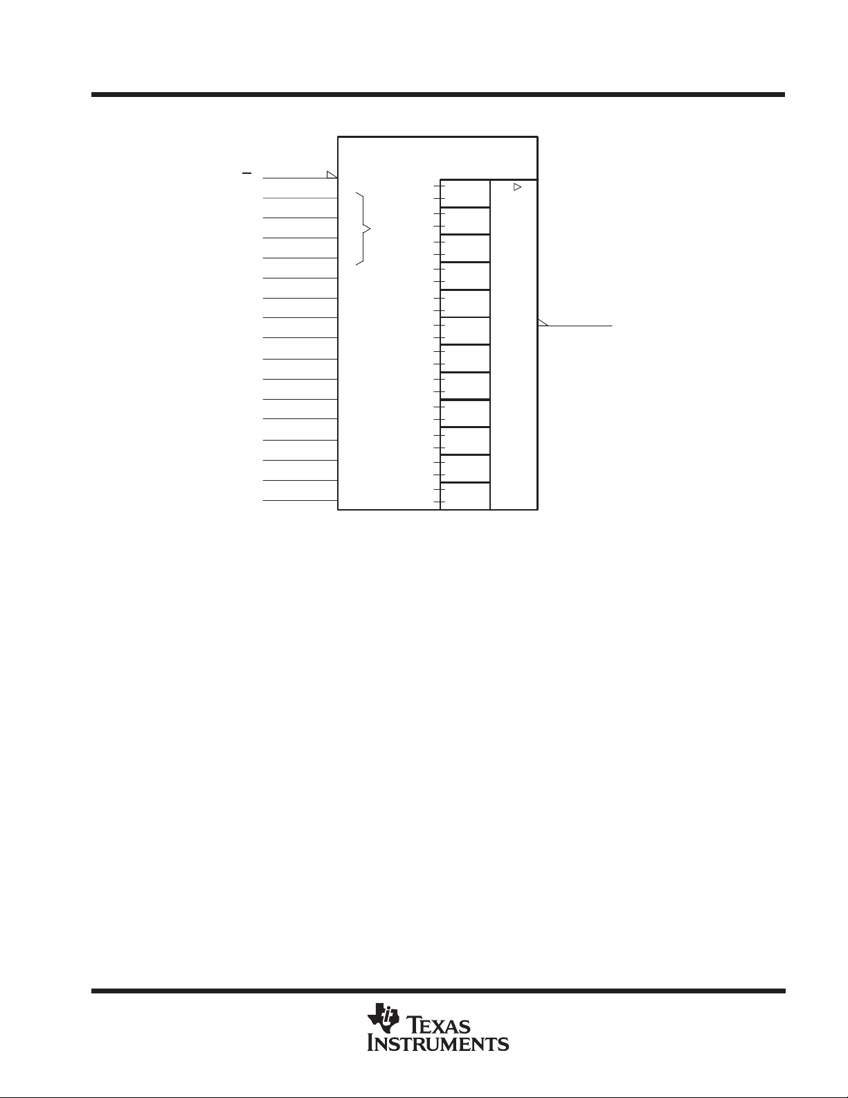
logic symbol
†
[ADDRESS COMP]
[P assumed ≠ 12, 13, 14]
EN
0
3
Z1
Z2
Z3
Z4
Z5
Z6
Z7
Z8
Z9
Z10
Z11
Z12
P
P ≥ 1
P ≥ 2
P ≥ 3
P ≥ 4
P ≥ 5
P ≥ 6
P ≥ 7
P ≥ 8
P ≥ 9
P ≥ 10
10
P ≥ 11
11
P ≥ 12
12
1
2
3
4
5
6
7
8
9
=1
=1
=1
=1
=1
=1
=1
=1
=1
=1
=1
=1
&
18
Y
P0
P1
P2
P3
A1
A2
A3
A4
A5
A6
A7
A8
A9
A10
A11
A12
19
G
14
15
16
17
1
2
3
4
5
6
7
8
9
11
12
13
†
This symbol is in accordance with ANSI/IEEE Std 91-1984 and IEC Publication 617-12.
2
POST OFFICE BOX 655303 • DALLAS, TEXAS 75265
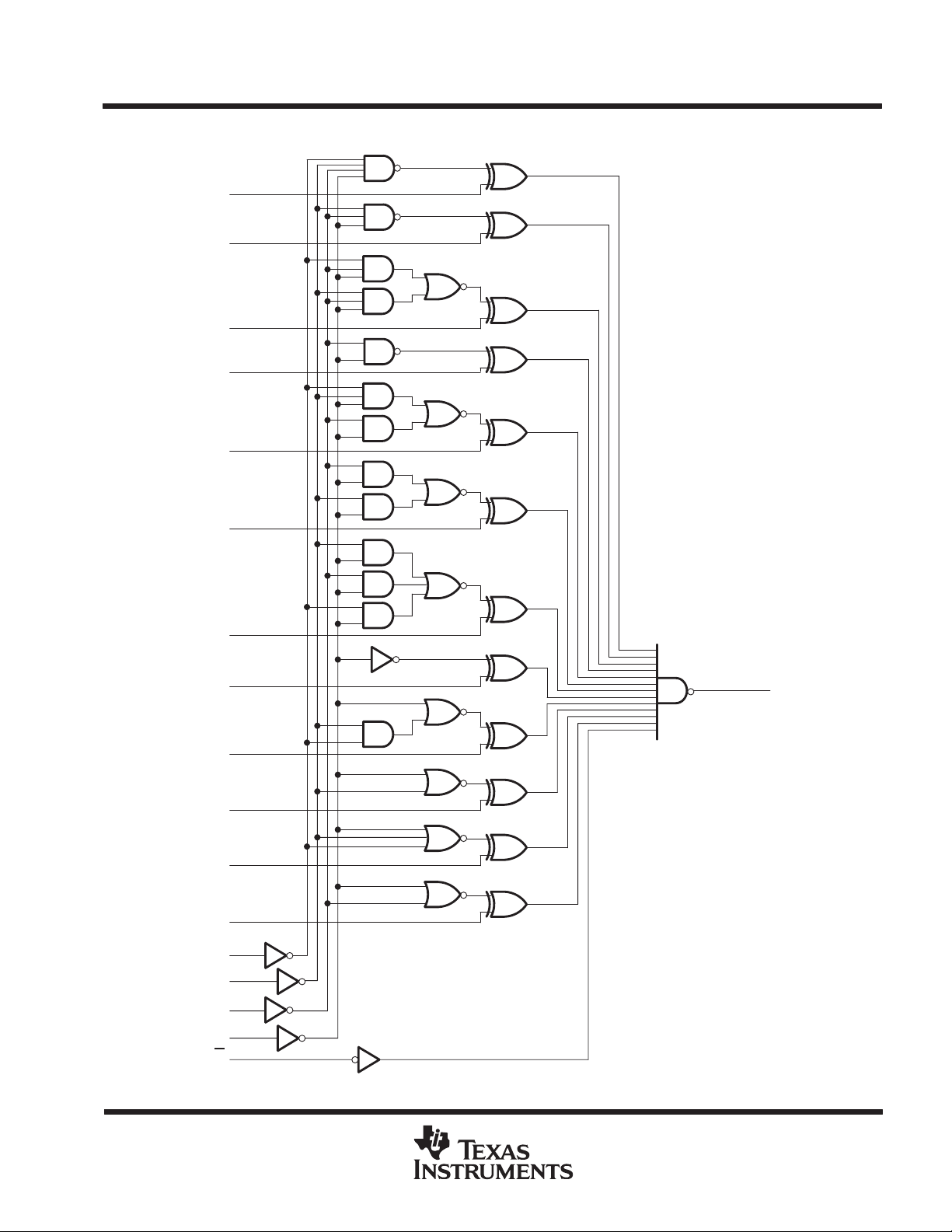
logic diagram (positive logic)
1
A1
2
A2
3
A3
4
A4
5
A5
SN74ALS679
12-BIT ADDRESS COMPARATOR
SDAS003C – JUNE 1982 – REVISED JANUARY 1995
A6
A7
A8
A9
A10
A11
A12
P0
P1
P2
P3
6
7
8
9
11
12
13
14
15
16
17
19
G
18
Y
POST OFFICE BOX 655303 • DALLAS, TEXAS 75265
3

SN74ALS679
V
V
VOLV
V
V
Any P
Y
ns
Any A
Y
ns
G
Y
ns
12-BIT ADDRESS COMPARATOR
SDAS003C – JUNE 1982 – REVISED JANUARY 1995
absolute maximum ratings over operating free-air temperature range (unless otherwise noted)
Supply voltage, V
Input voltage, V
Operating free-air temperature range, T
7 V. . . . . . . . . . . . . . . . . . . . . . . . . . . . . . . . . . . . . . . . . . . . . . . . . . . . . . . . . . . . . . . . . . . . . . . .
CC
7 V. . . . . . . . . . . . . . . . . . . . . . . . . . . . . . . . . . . . . . . . . . . . . . . . . . . . . . . . . . . . . . . . . . . . . . . . . . . .
I
0°C to 70°C. . . . . . . . . . . . . . . . . . . . . . . . . . . . . . . . . . . . . . . . . . . . . .
A
†
Storage temperature range –65°C to 150°C. . . . . . . . . . . . . . . . . . . . . . . . . . . . . . . . . . . . . . . . . . . . . . . . . . . . . . .
†
Stresses beyond those listed under “absolute maximum ratings” may cause permanent damage to the device. These are stress ratings only, and
functional operation of the device at these or any other conditions beyond those indicated under “recommended operating conditions” is not
implied. Exposure to absolute-maximum-rated conditions for extended periods may affect device reliability.
recommended operating conditions
MIN NOM MAX UNIT
V
V
V
I
I
T
CC
IH
IL
OH
OL
A
Supply voltage 4.5 5 5.5 V
High-level input voltage 2 V
Low-level input voltage 0.8 V
High-level output current –2.6 mA
Low-level output current 24 mA
Operating free-air temperature 0 70 °C
electrical characteristics over recommended operating free-air temperature range (unless
otherwise noted)
PARAMETER TEST CONDITIONS MIN TYP‡MAX UNIT
V
IK
OH
I
I
I
IH
I
IL
§
I
O
I
‡
All typical values are at VCC = 5 V, TA = 25°C.
§
The output conditions have been chosen to produce a current that closely approximates one half of the true short-circuit output current, IOS.
CC
VCC = 4.5 V, II = –18 mA –1.5 V
VCC = 4.5 V to 5.5 V, IOH = – 0.4 mA VCC –2
VCC = 4.5 V, IOH = – 2.6 mA 2.4 3.2
= 4.5
CC
VCC = 5.5 V, VI = 7 V 0.1 mA
VCC = 5.5 V, VI = 2.7 V 20 µA
VCC = 5.5 V, VI = 0.4 V –0.1 mA
VCC = 5.5 V, VO = 2.25 V –30 –112 mA
VCC = 5.5 V 17 28 mA
IOL = 12 mA 0.25 0.4
IOL = 24 mA 0.35 0.5
switching characteristics (see Figure 2)
VCC = 4.5 V to 5.5 V,
PARAMETER
t
PLH
t
PHL
t
PLH
t
PHL
t
PLH
t
¶
For conditions shown as MIN or MAX, use the appropriate value specified under recommended operating conditions.
4
PHL
FROM
(INPUT)
POST OFFICE BOX 655303 • DALLAS, TEXAS 75265
TO
(OUTPUT)
CL = 50 pF,
RL = 500 Ω,
TA = MIN to MAX
MIN MAX
4 25
8 35
5 22
5 30
3 13
5 25
UNIT
¶

SN74ALS679
12-BIT ADDRESS COMPARATOR
SDAS003C – JUNE 1982 – REVISED JANUARY 1995
APPLICATION INFORMATION
The SN74ALS679 can be wired to recognize any one of 212 addresses. The number of lows in the address determines
the input pattern for the P inputs. The system address lines that are low in the address to be recognized are connected
to the lowest-numbered A inputs of the address comparator. The system address lines that are high are connected
to the highest-numbered A inputs.
For example, assume the comparator is to enable a device when the 12-bit system address is:
A11 A10 A9 A8 A7 A6 A5 A4 A3 A2 A1 A0
H HLLHHLLHHHH
Because the address contains four lows and eight highs, the following connections are made:
• P3 to 0 V, P2 to V
, P1 to 0 V, and P0 to 0 V
CC
• System address lines A9, A8, A5, and A4 to comparator inputs A1 through A4 in any convenient order
• The remaining eight system address lines to comparator inputs A5 through A12 in any convenient order
The output provides an active-low enabling signal.
Figure 1 is a register-bank decoder that examines the 14 most significant bits (A0 through A13) of a 20-bit address
to select banks corresponding to the hex addresses 10000, 10040, 10080, and 100C0.
SN74ALS679
MEMEN
System
Address
Lines
A0 (MSB)–A19
A0–A2
A4–A11
A3
A12
A13
A14–A19
[ADDRESS
EN
0
3
COMP]
P
[P=11]
G
V
CC
11
6
P0
P1
P2
P3
A1–A11
A12
10000
10040
10080
100C0
G
16
16
16
16
A
B
0481216
=
=
=
=
1
2
LLLH
LLLH
LLLH
LLLH
′ALS139
LLLL
LLLL
LLLL
LLLL
1/2
X/Y
0
1
2
3
LLLL
LLLL
LLLL
LLLL
10000
10040
10080
100C0
S0–S5
LLLL
LHLL
HLLL
HHLL
16
16
16
16
LLLL
LLLL
LLLL
LLLL
64 X n-Bit
Registers
Figure 1. Register-Bank Decoder
POST OFFICE BOX 655303 • DALLAS, TEXAS 75265
5

SN74ALS679
12-BIT ADDRESS COMPARATOR
SDAS003C – JUNE 1982 – REVISED JANUARY 1995
PARAMETER MEASUREMENT INFORMATION
SERIES 54ALS/74ALS AND 54AS/74AS DEVICES
From Output
Under Test
(see Note A)
C
L
Test
Point
R
L
From Output
Under Test
C
(see Note A)
7 V
V
CC
S1
R
L
Test
Point
L
From Output
Under Test
(see Note A)
R1
C
L
RL = R1 = R2
Test
Point
R2
LOAD CIRCUIT FOR
BI-STATE
TOTEM-POLE OUTPUTS
Timing
Input
t
su
Data
Input
VOLTAGE WAVEFORMS
SETUP AND HOLD TIMES
Output
Control
(low-level
enabling)
Waveform 1
S1 Closed
(see Note B)
Waveform 2
S1 Open
(see Note B)
t
PZL
t
PZH
ENABLE AND DISABLE TIMES, 3-STATE OUTPUTS
VOLTAGE WAVEFORMS
1.3 V
t
PHZ
1.3 V
1.3 V
t
1.3 V1.3 V
1.3 V1.3 V
FOR OPEN-COLLECTOR OUTPUTS
h
t
PLZ
LOAD CIRCUIT
3.5 V
0.3 V
3.5 V
0.3 V
3.5 V
0.3 V
[
3.5 V
V
OL
0.3 V
V
OH
0.3 V
[
0 V
High-Level
Low-Level
Out-of-Phase
(see Note C)
Pulse
Pulse
Input
In-Phase
Output
Output
LOAD CIRCUIT
FOR 3-STATE OUTPUTS
1.3 V 1.3 V
t
w
1.3 V 1.3 V
VOLTAGE WAVEFORMS
PULSE DURATIONS
1.3 V 1.3 V
t
PLH
t
PHL
1.3 V 1.3 V
VOLTAGE WAVEFORMS
PROPAGATION DELAY TIMES
1.3 V1.3 V
t
PHL
t
PLH
3.5 V
0.3 V
3.5 V
0.3 V
3.5 V
0.3 V
V
V
V
V
OH
OL
OH
OL
NOTES: A. CL includes probe and jig capacitance.
B. Waveform 1 is for an output with internal conditions such that the output is low except when disabled by the output control.
Waveform 2 is for an output with internal conditions such that the output is high except when disabled by the output control.
C. When measuring propagation delay items of 3-state outputs, switch S1 is open.
D. All input pulses have the following characteristics: PRR ≤ 1 MHz, tr = tf = 2 ns, duty cycle = 50%.
E. The outputs are measured one at a time with one transition per measurement.
Figure 2. Load Circuits and Voltage Waveforms
6
POST OFFICE BOX 655303 • DALLAS, TEXAS 75265

IMPORTANT NOTICE
T exas Instruments and its subsidiaries (TI) reserve the right to make changes to their products or to discontinue
any product or service without notice, and advise customers to obtain the latest version of relevant information
to verify, before placing orders, that information being relied on is current and complete. All products are sold
subject to the terms and conditions of sale supplied at the time of order acknowledgement, including those
pertaining to warranty, patent infringement, and limitation of liability.
TI warrants performance of its semiconductor products to the specifications applicable at the time of sale in
accordance with TI’s standard warranty. Testing and other quality control techniques are utilized to the extent
TI deems necessary to support this warranty . Specific testing of all parameters of each device is not necessarily
performed, except those mandated by government requirements.
CERT AIN APPLICATIONS USING SEMICONDUCTOR PRODUCTS MAY INVOLVE POTENTIAL RISKS OF
DEATH, PERSONAL INJURY, OR SEVERE PROPERTY OR ENVIRONMENTAL DAMAGE (“CRITICAL
APPLICATIONS”). TI SEMICONDUCTOR PRODUCTS ARE NOT DESIGNED, AUTHORIZED, OR
WARRANTED TO BE SUITABLE FOR USE IN LIFE-SUPPORT DEVICES OR SYSTEMS OR OTHER
CRITICAL APPLICA TIONS. INCLUSION OF TI PRODUCTS IN SUCH APPLICATIONS IS UNDERST OOD TO
BE FULLY AT THE CUSTOMER’S RISK.
In order to minimize risks associated with the customer’s applications, adequate design and operating
safeguards must be provided by the customer to minimize inherent or procedural hazards.
TI assumes no liability for applications assistance or customer product design. TI does not warrant or represent
that any license, either express or implied, is granted under any patent right, copyright, mask work right, or other
intellectual property right of TI covering or relating to any combination, machine, or process in which such
semiconductor products or services might be or are used. TI’s publication of information regarding any third
party’s products or services does not constitute TI’s approval, warranty or endorsement thereof.
Copyright 1998, Texas Instruments Incorporated
 Loading...