Texas Instruments SN74ALS233BDW, SN74ALS233BDWR, SN74ALS233BFN, SN74ALS233BN Datasheet

SN74ALS233B
16 × 5 ASYNCHRONOUS FIRST-IN, FIRST-OUT MEMORY
SCAS253B – MARCH 1990 – REVISED APRIL 1998
1
POST OFFICE BOX 655303 • DALLAS, TEXAS 75265
D
Independent Asychronous Inputs and
Outputs
D
16 Words by 5 Bits
D
Data Rates From up to 40 MHz
D
Fall-Through Time 14 ns Typ
D
3-State Outputs
D
Package Options Include Plastic
Small-Outline Package (DW), Plastic Chip
Carriers (FN), and Standard Plastic 300-mil
DIPs (N)
description
This 80-bit memory uses advanced low-power
Schottky technology and features high speed and
a fast fall-through time. It is organized as 16 words
by 5 bits.
A FIFO memory is a storage device that allows
data to be written into and read from its array at
independent data rates. This FIFO is designed to
process data at rates up to 40 MHz in a bit-parallel
format, word by word.
Data is written into memory on a low-to-high
transition at the load clock (LDCK) input and is
read out on a low-to-high transition at the unload
clock (UNCK) input. The memory is full when the
number of words clocked in exceeds by 16 the
number of words clocked out. When the memory
is full, LDCK signals have no effect. When the
memory is empty, UNCK signals have no effect.
Status of the FIFO memory is monitored by the FULL
, EMPTY , FULL–1, and EMPTY+1 output flags. The FULL
output is low when the memory is full and high when it is not full. The FULL–1 output is low when the memory
contains 15 data words. The EMPTY
output is low when the memory is empty and high when it is not empty.
The EMPTY+1
output is low when one word remains in memory.
A low level on the reset (RST
) input resets the internal stack control pointers and also sets EMPTY low and sets
FULL
, FULL–1, and EMPTY+1 high. The Q outputs are not reset to any specific logic level. The first low-to-high
transition on LDCK, after either a RST
pulse or from an empty condition, causes EMPTY to go high and the data
to appear on the Q outputs. It is important to note that the first word does not have to be unloaded. Data outputs
are noninverting with respect to the data inputs and are at high impedance when the output-enable (OE) input
is low. OE does not af fect the output flags. Cascading is easily accomplished in the word-width direction but is
not possible in the word-depth direction.
The SN74ALS233B is characterized for operation from 0°C to 70°C.
Copyright 1998, Texas Instruments Incorporated
PRODUCTION DATA information is current as of publication date.
Products conform to specifications per the terms of Texas Instruments
standard warranty. Production processing does not necessarily include
testing of all parameters.
1
2
3
4
5
6
7
8
9
10
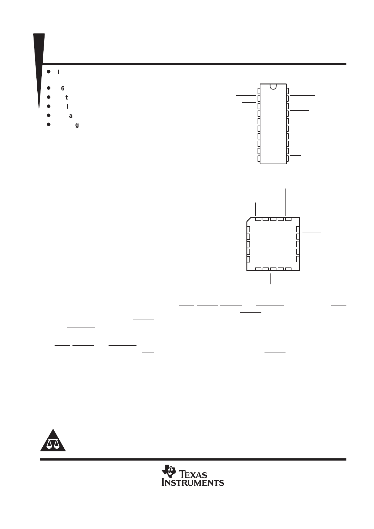
OE
FULL–1
FULL
LDCK
D0
D1
D2
D3
D4
GND
V
CC
EMPTY+1
UNCK
EMPTY
Q0
Q1
Q2
Q3
Q4
RST
DW OR N PACKAGE
(TOP VIEW)
3212019
910111213
4
5
6
7
8
UNCK
EMPTY
Q0
Q1
Q2
LDCK
D0
D1
D2
D3
FN PACKAGE
(TOP VIEW)
FULL
FULL–1
OE
Q4
Q3
EMPTY+1
D4
GND
RST
V
CC
20
19
18
17
16
15
14
13
12
11
18
17
16
15
14
Please be aware that an important notice concerning availability, standard warranty, and use in critical applications of
Texas Instruments semiconductor products and disclaimers thereto appears at the end of this data sheet.

SN74ALS233B
16 × 5 ASYNCHRONOUS FIRST -IN, FIRST-OUT MEMORY
SCAS253B – MARCH 1990 – REVISED APRIL 1998
2
POST OFFICE BOX 655303 • DALLAS, TEXAS 75265
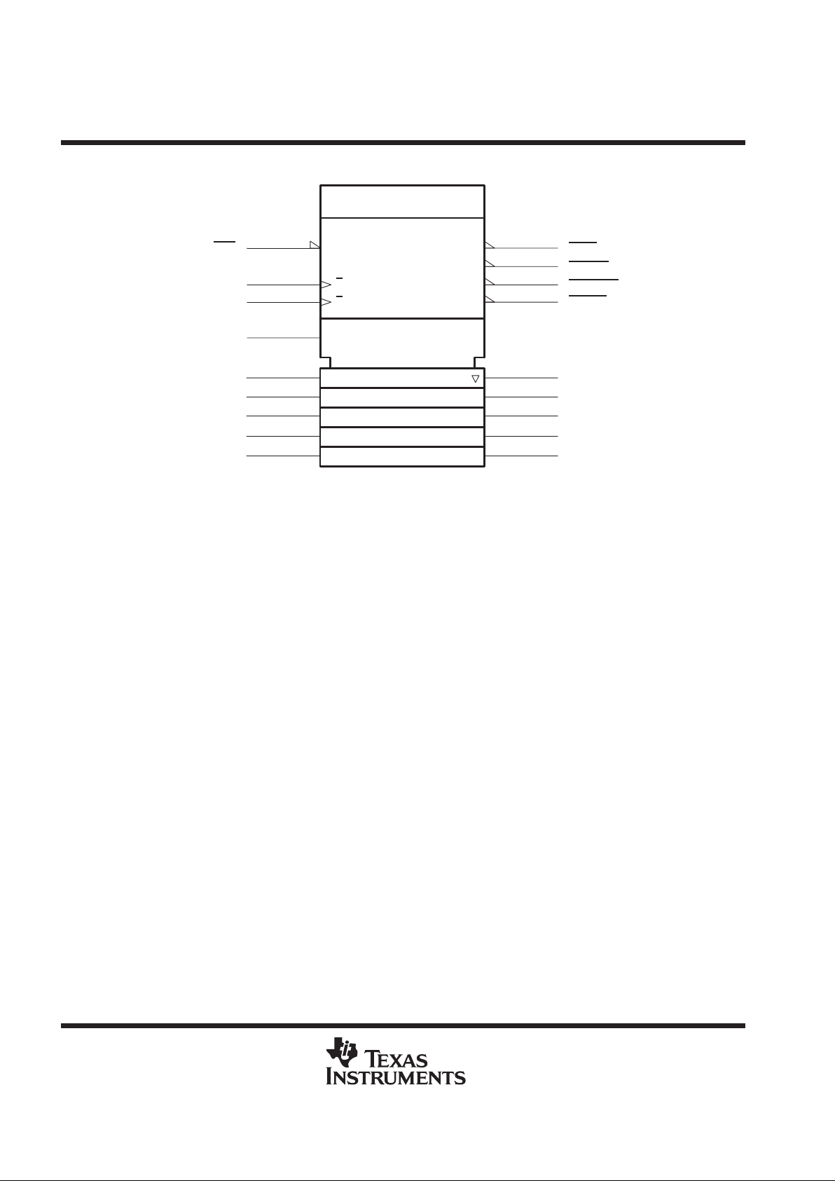
logic symbol
†
CT = 0
11
EN4
1
OE
2D
5
D0
17
(CT = 0) G3
Q0
16
6
D1
Q1
15
7
D2
Q2
14
8
D3
Q3
13
9
D4
Q4
12
18
UNCK
19
CT = 1
2
CT = 15
3
(CT = 16) G1
4
LDCK
FIFO 16 × 5
(ALS233B)
CTR
RST
FULL
FULL–1
EMPTY+1
EMPTY
3–
1
(+/C2)
4
†
This symbol is in accordance with ANSI/IEEE Standard 91-1984 and IEC Publication 617-12. The symbol is functionally accurate but does
not show the details of implementation; for these, see the logic diagram. The symbol represents the memory as if it were controlled by a single
counter whose content is the number of words stored at the time. Output data is invalid when the counter content (CT) is 0.

SN74ALS233B
16 × 5 ASYNCHRONOUS FIRST -IN, FIRST-OUT MEMORY
SCAS253B – MARCH 1990 – REVISED APRIL 1998
3
POST OFFICE BOX 655303 • DALLAS, TEXAS 75265
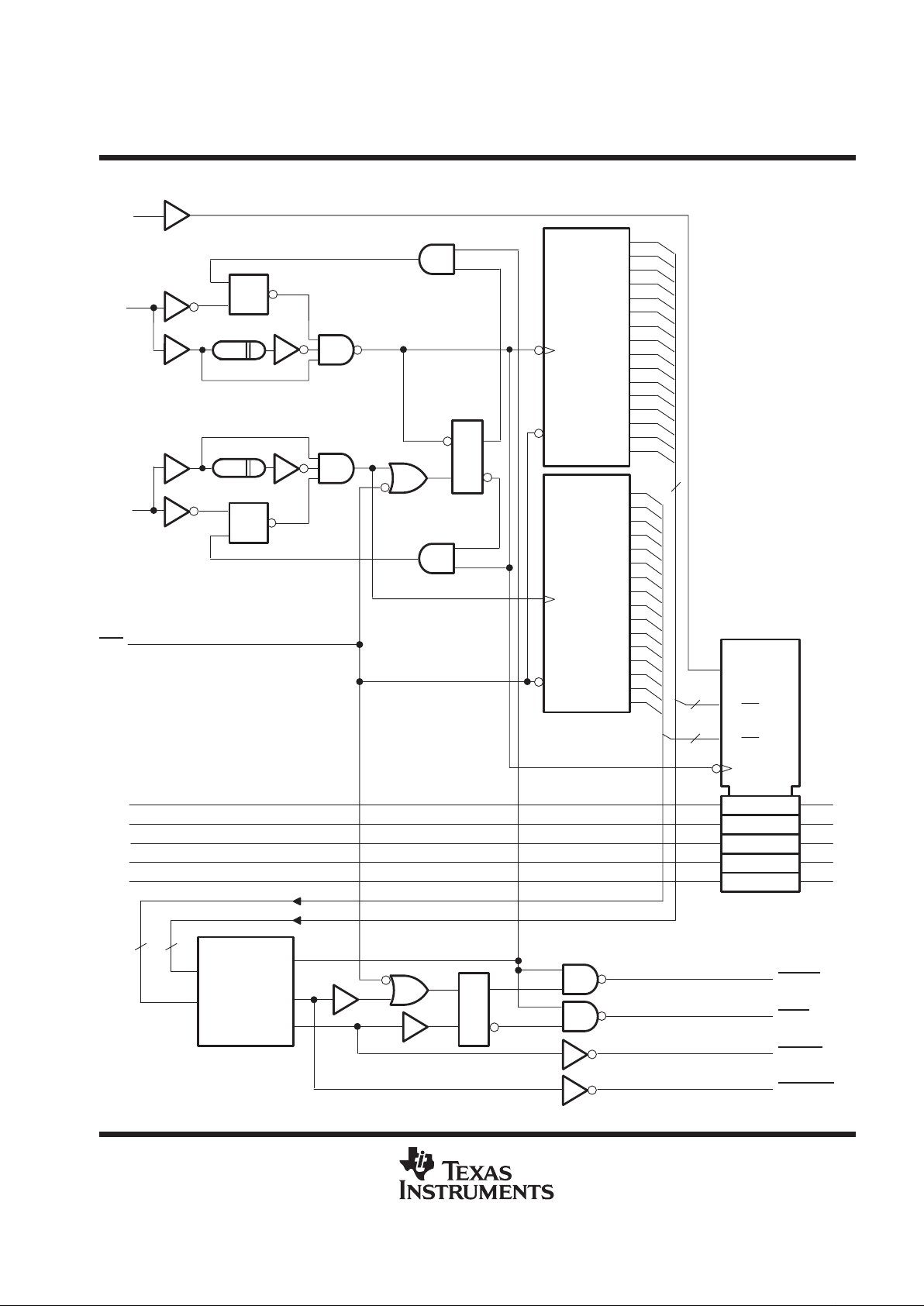
logic diagram (positive logic)
1A, 3D
5
D0
6
D1
7
D2
8
D3
9
D4
Q0
16
2A
Q1
15
Q2
14
Q3
13
Q4
12
C3
EN
3
2
19
17
FULL
FULL–1
EMPTY+1
EMPTY
RAM 16 × 5
1A
16
2A
16
1
16
1
16
7
8
9
10
11
12
13
14
15
16
1
2
3
4
5
6
+
CT = 1
COMP
P = Q
P = Q + 2
P = Q – 2
P
Q
1616
S
R
7
8
9
10
11
12
13
14
15
16
1
2
3
4
5
6
+
CT = 1
18
UNCK
C1
1D
S
R
4
LDCK
C1
1D
11
RST
1
OE
Ring
Counter
CTR
DIV 16
Write
Address
Read
Address
16
Ring
Counter
CTR
DIV 16
 Loading...