

Datasheet SN74ALS232BDW, SN74ALS232BDWR, SN74ALS232BFN, SN74ALS232BFNR, SN74ALS232BN Datasheet (Texas Instruments)
SN74ALS232B
16 × 4 ASYNCHRONOUS FIRST-IN, FIRST-OUT MEMORY
SCAS251B – FEBRUARY 1989 – REVISED APRIL 1998
1
POST OFFICE BOX 655303 • DALLAS, TEXAS 75265
D
Independent Asynchronous Inputs and
Outputs
D
16 Words by 4 Bits
D
Data Rates up to 40 MHz
D
Fall-Through Time 14 ns Typical
D
3-State Outputs
D
Package Options Include Plastic
Small-Outline Package (DW), Plastic Chip
Carriers (FN), and Standard Plastic 300-mil
DIPs (N)
description
This 64-bit memory features high speed and fast
fall-through times. It is organized as 16 words by
4 bits.
A first-in, first-out (FIFO) memory is a storage
device that allows data to be written into and read
from its array at independent data rates. This
FIFO is designed to process data at rates up to
40 MHz in a bit-parallel format, word by word.
Data is written into memory on a low-to-high
transition at the load-clock (LDCK) input and is
read out on a low-to-high transition at the
unload-clock (UNCK) input. The memory is full
when the number of words clocked in exceeds by
16 the number of words clocked out. When the
memory is full, LDCK signals have no effect on the
data residing in memory. When the memory is
empty, UNCK signals have no effect.
Status of the FIFO memory is monitored by the FULL
and EMPTY output flags. The FULL output is low when
the memory is full and high when it is not full. The EMPTY
output is low when the memory is empty and high
when it is not empty.
A low level on the reset (RST
) input resets the internal stack-control pointers and also sets EMPTY low and sets
FULL
high. The Q outputs are not reset to any specific logic level. The first low-to-high transition on LDCK, after
either a RST
pulse or from an empty condition, causes EMPTY to go high and the data to appear on the
Q outputs. It is important to note that the first word does not have to be unloaded. Data outputs are noninverting
with respect to the data inputs and are at high impedance when the output-enable (OE) input is low. OE does
not affect the FULL
or EMPTY output flags. Cascading is easily accomplished in the word-width direction but
is not possible in the word-depth direction.
The SN74ALS232B is characterized for operation from 0°C to 70°C.
Copyright 1998, Texas Instruments Incorporated
PRODUCTION DATA information is current as of publication date.
Products conform to specifications per the terms of Texas Instruments
standard warranty. Production processing does not necessarily include
testing of all parameters.
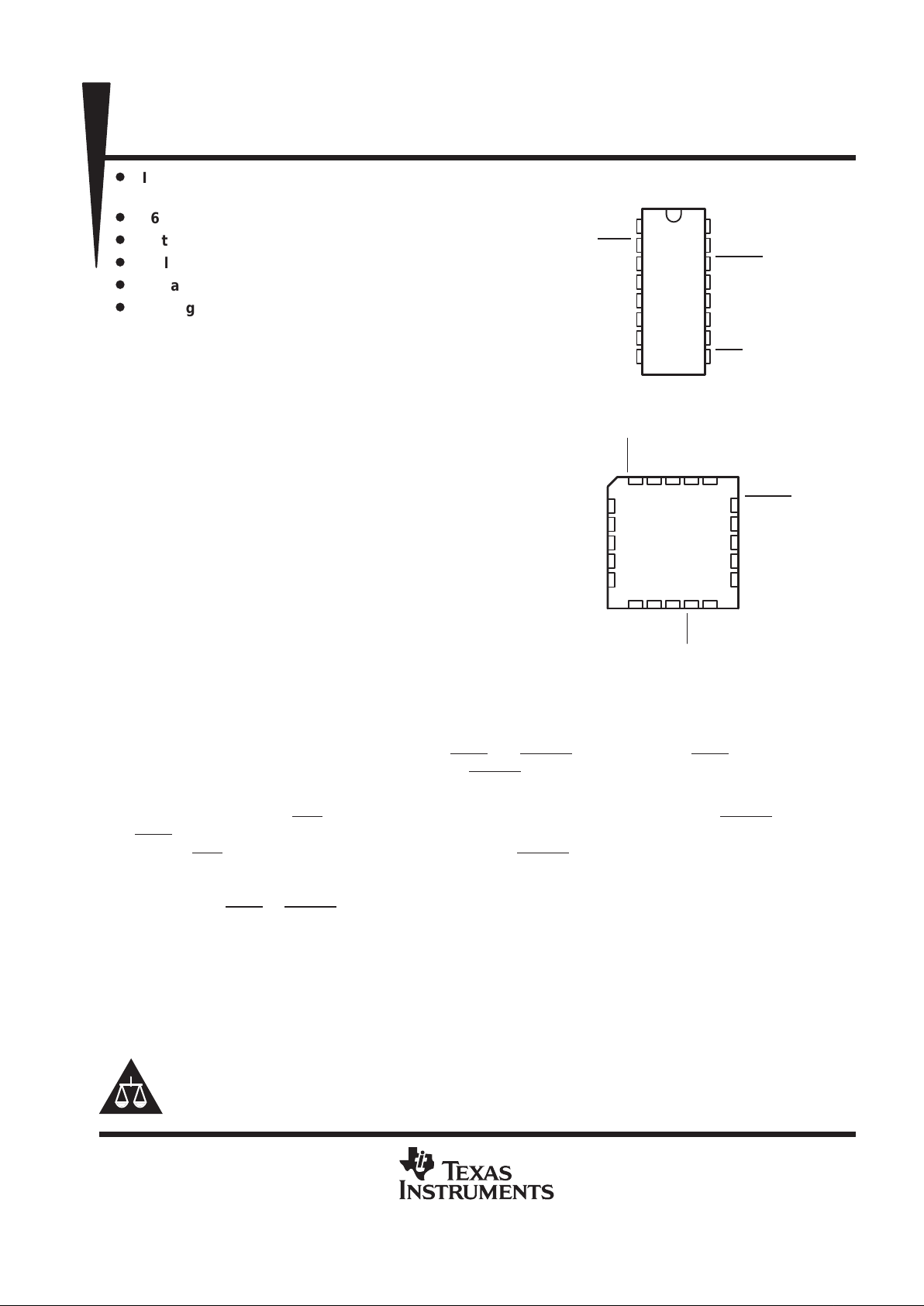
OE
FULL
LDCK
D0
D1
D2
D3
GND
DW OR N PACKAGE
(TOP VIEW)
3 2 1 20 19
910111213
4
5
6
7
8
18
17
16
15
14
EMPTY
Q0
NC
Q1
Q2
LDCK
D0
NC
D1
D2
FN PACKAGE
(TOP VIEW)
OE
NC
RST
Q3
UNCK
D3
GND
NC
V
CC
FULL
1
2
3
4
5
6
7
8
16
15
14
13
12
11
10
9
V
CC
UNCK
EMPTY
Q0
Q1
Q2
Q3
RST
NC – No internal connection
Please be aware that an important notice concerning availability, standard warranty, and use in critical applications of
Texas Instruments semiconductor products and disclaimers thereto appears at the end of this data sheet.
SN74ALS232B
16 × 4 ASYNCHRONOUS FIRST -IN, FIRST-OUT MEMORY
SCAS251B – FEBRUARY 1989 – REVISED APRIL 1998
2
POST OFFICE BOX 655303 • DALLAS, TEXAS 75265
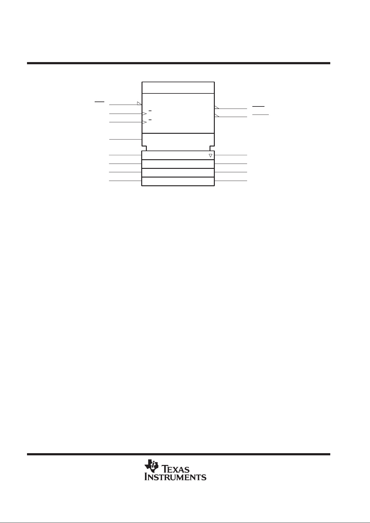
logic symbol
†
CT = 0
9
EN4
1
OE
2D
4
D0 Q0
13
5
D1
Q1
12
6
D2
Q2
11
7
D3
Q3
10
15
UNCK
14
(CT = 0) G3
2
(CT = 16) G1
3
LDCK
FIFO 16 × 4
CTR
RST
FULL
EMPTY
3–
1
(+/C2)
4
†
This symbol is in accordance with ANSI/IEEE Standard 91-1984 and IEC Publication 617-12. The symbol is functionally accurate but does
not show the details of implementation; for these, see the logic diagram. The symbol represents the memory as if it were controlled by a single
counter whose content is the number of words stored at the time. Output data is invalid when the counter content (CT) is 0.
Pin numbers shown are for the DW and N packages.
SN74ALS232B
16 × 4 ASYNCHRONOUS FIRST -IN, FIRST-OUT MEMORY
SCAS251B – FEBRUARY 1989 – REVISED APRIL 1998
3
POST OFFICE BOX 655303 • DALLAS, TEXAS 75265
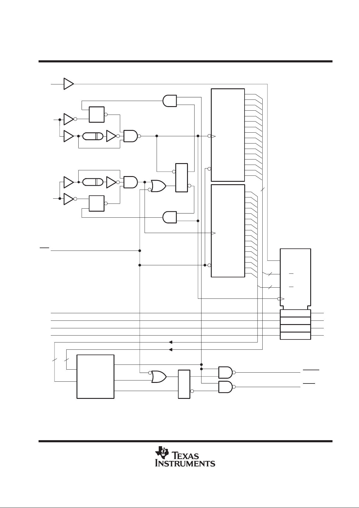
logic diagram (positive logic)
1A, 3D
4
D0
5
D1
6
D2
7
D3
Q0
13
2A
Q1
12
Q2
11
Q3
10
C3
EN
2
14
FULL
EMPTY
RAM 16 × 4
1A
16
2A
16
1
16
1
16
7
8
9
10
11
12
13
14
15
16
1
2
3
4
5
6
+
CT = 1
COMP
P = Q
P= Q+1
P = Q–1
P
Q
1616
S
R
7
8
9
10
11
12
13
14
15
16
1
2
3
4
5
6
+
CT = 1
15
UNCK
C2
2D
S
R
3
LDCK
C1
1D
9
RST
1
OE
Ring
Counter
CTR
DIV 16
Ring
Counter
CTR
DIV 16
Write
Address
Read
Address
16
Pin numbers shown are for the DW and N packages.

SN74ALS232B
16 × 4 ASYNCHRONOUS FIRST -IN, FIRST-OUT MEMORY
SCAS251B – FEBRUARY 1989 – REVISED APRIL 1998
4
POST OFFICE BOX 655303 • DALLAS, TEXAS 75265
timing diagram
Invalid
Invalid
Word 1Word 1
Word 2 Word 3
RST
LDCK
D0–D3
UNCK
Q0–Q3
EMPTY
FULL
W1 W2 W3
Don’t Care
W1 W2 W15 W16
Word 2 Word 3 Word 4
Initialize
Pointers
Load
W1
Unload
W2
Empty Full
absolute maximum ratings over operating free-air temperature range (unless otherwise noted)
†
Supply voltage range, V
CC
–0.5 V to 7 V. . . . . . . . . . . . . . . . . . . . . . . . . . . . . . . . . . . . . . . . . . . . . . . . . . . . . . . . . .
Input voltage range, V
I
–0.5 V to 7 V. . . . . . . . . . . . . . . . . . . . . . . . . . . . . . . . . . . . . . . . . . . . . . . . . . . . . . . . . . . . . .
Voltage range applied to a disabled 3-state output –0.5 V to 5.5 V. . . . . . . . . . . . . . . . . . . . . . . . . . . . . . . . . . . . .
Package thermal impedance, θ
JA
(see Note 2): DW package 105°C/W. . . . . . . . . . . . . . . . . . . . . . . . . . . . . . . .
FN package 83°C/W. . . . . . . . . . . . . . . . . . . . . . . . . . . . . . . . .
N package 78°C/W. . . . . . . . . . . . . . . . . . . . . . . . . . . . . . . . . . .
Storage temperature range, T
stg
–65°C to 150°C. . . . . . . . . . . . . . . . . . . . . . . . . . . . . . . . . . . . . . . . . . . . . . . . . . .
†
Stresses beyond those listed under “absolute maximum ratings” may cause permanent damage to the device. This is a stress rating only, and
functional operation of the device at these or any other conditions beyond those indicated in the “recommended operating conditions” section of
this specification is not implied. Exposure to absolute-maximum-rated conditions for extended periods may affect device reliability.
NOTES: 1. All voltage values are with respect to GND.
2. The package thermal impedance is calculated in accordance with JESD 51, except for through-hole packages, which use a trace
length of zero.

SN74ALS232B
16 × 4 ASYNCHRONOUS FIRST -IN, FIRST-OUT MEMORY
SCAS251B – FEBRUARY 1989 – REVISED APRIL 1998
5
POST OFFICE BOX 655303 • DALLAS, TEXAS 75265
recommended operating conditions (see Note 3)
MIN NOM MAX UNIT
V
CC
Supply voltage 4.5 5 5.5 V
V
IH
High-level input voltage 2 V
V
IL
Low-level input voltage 0.8 V
p
Q outputs –2.6
IOHHigh-level output current
FULL, EMPTY –0.4
mA
p
Q outputs 24
IOLLow-level output current
FULL, EMPTY 8
mA
T
A
Operating free-air temperature 0 70 °C
NOTE 3: T o ensure proper operation of this high-speed FIFO device, it is necessary to provide a clean signal to the LDCK and UNCK clock inputs.
Any excessive noise or glitching on the clock inputs that violates limits for maximum VIL, minimum VIH, or minimum pulse duration can
cause a false clock or improper operation of the internal read and write pointers.
electrical characteristics over recommended operating free-air temperature range (unless
otherwise noted)
PARAMETER TEST CONDITIONS MIN TYP†MAX UNIT
V
IK
VCC = 4.5 V, II = –18 mA –1.2 V
Q outputs VCC = 4.5 V, IOH = –2.6 mA 2.4 3.2
V
OH
FULL, EMPTY VCC = 4.5 V to 5.5 V, IOH = –0.4 mA VCC–2
V
p
IOL = 12 mA 0.25 0.4
Q outputs
V
CC
= 4.5
V
IOL = 24 mA 0.35 0.5
V
OL
IOL = 4 mA 0.25 0.4
V
FULL, EMPTY
V
CC
=
4.5 V
IOL = 8 mA 0.35 0.5
I
OZH
VCC = 5.5 V, VO = 2.7 V 20 µA
I
OZL
VCC = 5.5 V, VO = 0.4 V –20 µA
I
I
VCC = 5.5 V, VI = 7 V 0.1 mA
I
IH
VCC = 5.5 V, VI = 2.7 V 20 µA
I
IL
VCC = 5.5 V, VI = 0.4 V –0.2 mA
I
O
‡
VCC = 5.5 V, VO = 2.25 V –30 –112 mA
I
CC
VCC = 5.5 V 80 125 mA
†
All typical values are at VCC = 5 V, TA = 25°C.
‡
The output conditions have been chosen to produce a current that closely approximates one-half of the true short-circuit output current, IOS.

SN74ALS232B
16 × 4 ASYNCHRONOUS FIRST -IN, FIRST-OUT MEMORY
SCAS251B – FEBRUARY 1989 – REVISED APRIL 1998
6
POST OFFICE BOX 655303 • DALLAS, TEXAS 75265
timing requirements over recommended operating free-air temperature range (see Figure 1)
MIN NOM MAX UNIT
LDCK 40
f
clock
†
Clock frequenc
y
UNCK
40
MH
z
RST low 18
LDCK low 15
t
w
Pulse duration
LDCK high
10
ns
UNCK low 15
UNCK high 10
p
Data before LDCK↑ 8
tsuSetup time
LDCK inactive before RST↑ 5
ns
Data after LDCK↑ 5
thHold time
LDCK inactive after RST↑ 5
ns
†
The maximum possible clock frequency is 40 MHz. The maximum clock frequency when using a 50% duty cycle is 33.3 MHz.
switching characteristics (see Figure 1)
PARAMETER
FROM
(INPUT)
TO
(OUTPUT)
MIN TYP‡MAX MIN MAX UNIT
f
max
LDCK, UNCK 50 40 MHz
LDCK↑
14 23 6 30
t
pd
UNCK↑
Any Q
15 23 6 30
ns
t
PLH
LDCK↑
EMPTY
13 20 5 25 ns
UNCK↑
15 22 6 27
t
PHL
RST↓
EMPTY
15 21 5 26
ns
LDCK↑ FULL 15 22 6 27
UNCK↑
13 20 5 25
t
PLH
RST↓
FULL
16 23 7 28
ns
t
en
OE↑ Q 5 12 1 14 ns
t
dis
OE↓ Q 5 12 1 16 ns
‡
Typical values at VCC – 5 V, TA = 25°C.

SN74ALS232B
16 × 4 ASYNCHRONOUS FIRST -IN, FIRST-OUT MEMORY
SCAS251B – FEBRUARY 1989 – REVISED APRIL 1998
7
POST OFFICE BOX 655303 • DALLAS, TEXAS 75265
PARAMETER MEASUREMENT INFORMATION
t
PHZ
t
PLZ
t
PHL
t
PLH
0.3 V
t
PZL
t
PZH
t
PLH
t
PHL
LOAD CIRCUIT FOR 3-STATE OUTPUTS
From Output
Under Test
Test Point
R1 = 500 Ω
S1
CL = 50 pF
7 V
(see Note A)
Open
1.3 V
1.3 V1.3 V
3.5 V
3.5 V
0.3 V
0.3 V
t
h
t
su
VOLTAGE WAVEFORMS
SETUP AND HOLD TIMES
Timing
Input
Data
Input
1.3 V 1.3 V
3.5 V
3.5 V
0.3 V
0.3 V
High-Level
Pulse
Low-Level
Pulse
VOLTAGE WAVEFORMS
PULSE DURATION
Input
(see Note C)
Out-of-Phase
Output
1.3 V 1.3 V
1.3 V1.3 V
1.3 V 1.3 V
1.3 V1.3 V
1.3 V
1.3 V
3.5 V
3.5 V
0.3 V
0.3 V
V
OL
V
OH
V
OH
V
OL
Output
Control
Waveform 1
S1 Closed
(see Note B)
Waveform 2
S1 Open
(see Note B)
0 V
V
OH
V
OL
3.5 V
In-Phase
Output
0.3 V
1.3 V 1.3 V
VOLTAGE WAVEFORMS
PROPAGATION DELAY TIMES
VOLTAGE WAVEFORMS
ENABLE AND DISABLE TIMES, 3-STATE OUTPUTS
SWITCH POSITION TABLE
R2 = 500 Ω
t
w
NOTES: A. CL includes probe and jig capacitance.
B. Waveform 1 is for an output with internal conditions such that the output is low except when disabled by the output control.
Waveform 2 is for an output with internal conditions such that the output is high except when disabled by the output control.
C. All input pulses are supplied by generators having the following characteristics: PRR ≤ 1 MHz, Zo = 50 Ω, tr ≤ 2 ns, tf≤ 2 ns.
D. The outputs are measured one at a time with one transition per measurement.
t
PZH
t
PZL
t
PHZ
t
PLZ
t
PLH
t
PHL
Open
Closed
Open
Closed
Open
Open
PARAMETER S1
t
en
t
dis
t
pd
Figure 1. Load Circuit and Voltage Waveforms

IMPORTANT NOTICE
T exas Instruments and its subsidiaries (TI) reserve the right to make changes to their products or to discontinue
any product or service without notice, and advise customers to obtain the latest version of relevant information
to verify, before placing orders, that information being relied on is current and complete. All products are sold
subject to the terms and conditions of sale supplied at the time of order acknowledgement, including those
pertaining to warranty, patent infringement, and limitation of liability.
TI warrants performance of its semiconductor products to the specifications applicable at the time of sale in
accordance with TI’s standard warranty. Testing and other quality control techniques are utilized to the extent
TI deems necessary to support this warranty. Specific testing of all parameters of each device is not necessarily
performed, except those mandated by government requirements.
CERT AIN APPLICATIONS USING SEMICONDUCTOR PRODUCTS MA Y INVOLVE POTENTIAL RISKS OF
DEATH, PERSONAL INJURY, OR SEVERE PROPERTY OR ENVIRONMENTAL DAMAGE (“CRITICAL
APPLICATIONS”). TI SEMICONDUCTOR PRODUCTS ARE NOT DESIGNED, AUTHORIZED, OR
WARRANTED TO BE SUITABLE FOR USE IN LIFE-SUPPORT DEVICES OR SYSTEMS OR OTHER
CRITICAL APPLICATIONS. INCLUSION OF TI PRODUCTS IN SUCH APPLICA TIONS IS UNDERST OOD TO
BE FULLY AT THE CUSTOMER’S RISK.
In order to minimize risks associated with the customer’s applications, adequate design and operating
safeguards must be provided by the customer to minimize inherent or procedural hazards.
TI assumes no liability for applications assistance or customer product design. TI does not warrant or represent
that any license, either express or implied, is granted under any patent right, copyright, mask work right, or other
intellectual property right of TI covering or relating to any combination, machine, or process in which such
semiconductor products or services might be or are used. TI’s publication of information regarding any third
party’s products or services does not constitute TI’s approval, warranty or endorsement thereof.
Copyright 1998, Texas Instruments Incorporated
 Loading...