

Texas Instruments SN74ALS165D, SN74ALS165DR, SN74ALS165N, SN74ALS165N3, SNJ54ALS165FK Datasheet
...
SN54ALS165, SN74ALS165
PARALLEL-LOAD 8-BIT REGISTERS
SDAS157B – JUNE 1982 – REVISED DECEMBER 1994
Copyright 1994, Texas Instruments Incorporated
1
POST OFFICE BOX 655303 • DALLAS, TEXAS 75265
• Complementary Outputs
• Direct Overriding Load (Data) Inputs
• Gated Clock Inputs
• Parallel-to-Serial Data Conversion
• Package Options Include Plastic
Small-Outline (D) Packages, Ceramic Chip
Carriers (FK), and Standard Plastic (N) and
Ceramic (J) 300-mil DIPs
description
The ′ALS165 are parallel-load 8-bit serial shift
registers that, when clocked, shift the data toward
serial (Q
H
and QH) outputs. Parallel-in access to
each stage is provided by eight individual direct
data (A–H) inputs that are enabled by a low level
at the shift/load (SH/LD
) input. The ′ALS165 have
a clock-inhibit function and complemented serial
outputs.
Clocking is accomplished by a low-to-high
transition of the clock (CLK) input while SH/LD
is
held high and the clock inhibit (CLK INH) input is
held low. The functions of CLK and CLK INH are
interchangeable. Since a low CLK and a
low-to-high transition of CLK INH also
accomplishes clocking, CLK INH should be
changed to the high level only while CLK is high.
Parallel loading is inhibited when SH/LD
is held
high. The parallel inputs to the register are
enabled while SH/LD
is low independently of the
levels of the CLK, CLK INH, or serial (SER) inputs.
The SN54ALS165 is characterized for operation over the full military temperature range of –55°C to 125°C. The
SN74ALS165 is characterized for operation from 0°C to 70°C.
FUNCTION TABLE
INPUTS
SH/LD
CLK CLK INH
FUNCTION
L X X Parallel load
H H X No change
H X H No change
H L ↑ Shift
†
H ↑ L Shift
†
†
Shift = content of each internal register shifts
toward serial outputs. Data at SER is shifted
into first register.
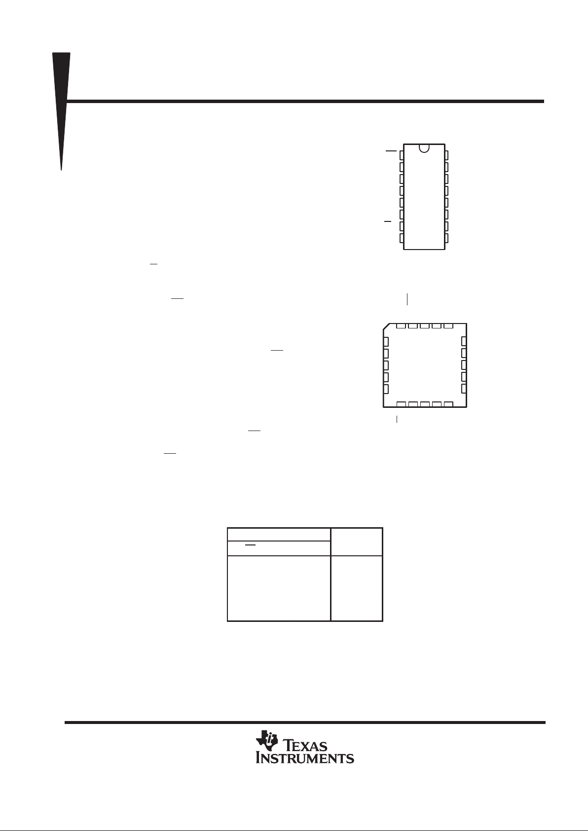
SN54ALS165 ...J PACKAGE
SN74ALS165 ...D OR N PACKAGE
(TOP VIEW)
3212019
910111213
4
5
6
7
8
18
17
16
15
14
D
C
NC
B
A
E
F
NC
G
H
SN54ALS165 . . . FK PACKAGE
(TOP VIEW)
CLK
SH/LD
NC
SER
CLK INH
H
GND
NC
NC – No internal connection
V
CC
1
2
3
4
5
6
7
8
16
15
14
13
12
11
10
9
SH/LD
CLK
E
F
G
H
Q
H
GND
V
CC
CLK INH
D
C
B
A
SER
Q
H
Q
H
Q
PRODUCTION DATA information is current as of publication date.
Products conform to specifications per the terms of Texas Instruments
standard warranty. Production processing does not necessarily include
testing of all parameters.
SN54ALS165, SN74ALS165
PARALLEL-LOAD 8-BIT REGISTERS
SDAS157B – JUNE 1982 – REVISED DECEMBER 1994
2
POST OFFICE BOX 655303 • DALLAS, TEXAS 75265
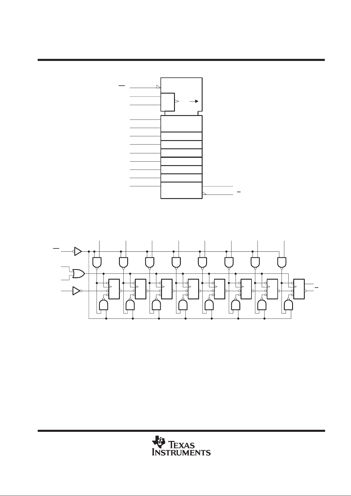
logic symbol
†
SRG8
C1 [LOAD]
1
15
CLK INH
2
CLK
14
D
2D
10
SER
1D
11
A
1D
12
B
13
C
3
E
4
F
5
G
1D
6
H
C2/
7
9
≥1
SH/LD
Q
H
Q
H
†
This symbol is in accordance with ANSI/IEEE Std 91-1984 and IEC Publication 617-12.
Pin numbers shown are for the D, J, and N packages.
logic diagram (positive logic)
S
1D
R
C1
S
1D
R
C1
S
1D
R
C1
S
1D
R
C1
S
1D
R
C1
S
1D
R
C1
S
1D
R
C1
S
1D
R
C1
1
15
2
10
SH/LD
CLK INH
CLK
SER
9
7
Q
H
Q
H
11 12 13 14 3 4 5 6
ABCDEFGH
Pin numbers shown are for the D, J, and N packages.
SN54ALS165, SN74ALS165
PARALLEL-LOAD 8-BIT REGISTERS
SDAS157B – JUNE 1982 – REVISED DECEMBER 1994
3
POST OFFICE BOX 655303 • DALLAS, TEXAS 75265
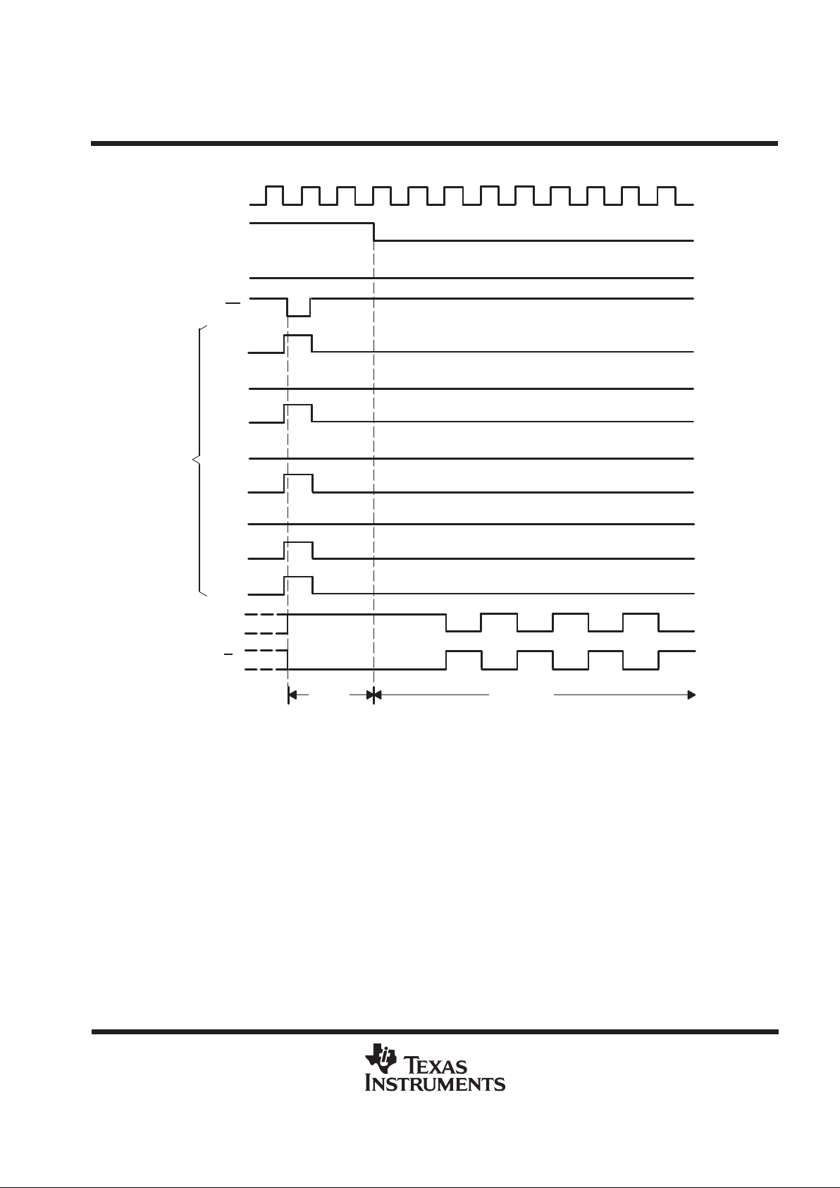
typical shift, load, and inhibit sequences
Load
E
Q
H
H
G
C
F
Data
Inputs
D
SH/LD
SER
CLK INH
CLK
B
A
Q
H
L
L
H
L
H
L
H
H
H
H
L
H
L
H
L
H
L
H
L
L
H
L
H
L
H
Inhibit Serial Shift
absolute maximum ratings over operating free-air temperature range (unless otherwise noted)
†
Supply voltage, V
CC
7 V. . . . . . . . . . . . . . . . . . . . . . . . . . . . . . . . . . . . . . . . . . . . . . . . . . . . . . . . . . . . . . . . . . . . . . . .
Input voltage, V
I
7 V. . . . . . . . . . . . . . . . . . . . . . . . . . . . . . . . . . . . . . . . . . . . . . . . . . . . . . . . . . . . . . . . . . . . . . . . . . . .
Operating free-air temperature range, T
A
: SN54ALS165 –55°C to 125°C. . . . . . . . . . . . . . . . . . . . . . . . . . . . .
SN74ALS165 0°C to 70°C. . . . . . . . . . . . . . . . . . . . . . . . . . . . . . . . .
Storage temperature range –65°C to 150°C. . . . . . . . . . . . . . . . . . . . . . . . . . . . . . . . . . . . . . . . . . . . . . . . . . . . . . .
†
Stresses beyond those listed under “absolute maximum ratings” may cause permanent damage to the device. These are stress ratings only, and
functional operation of the device at these or any other conditions beyond those indicated under “recommended operating conditions” is not
implied. Exposure to absolute-maximum-rated conditions for extended periods may affect device reliability.

SN54ALS165, SN74ALS165
PARALLEL-LOAD 8-BIT REGISTERS
SDAS157B – JUNE 1982 – REVISED DECEMBER 1994
4
POST OFFICE BOX 655303 • DALLAS, TEXAS 75265
recommended operating conditions
SN54ALS165 SN74ALS165
MIN NOM MAX MIN NOM MAX
UNIT
V
CC
Supply voltage 4.5 5 5.5 4.5 5 5.5 V
V
IH
High-level input voltage 2 2 V
V
IL
Low-level input voltage 0.7 0.8 V
I
OH
High-level output current –0.4 –0.4 mA
I
OL
Low-level output current 4 8 mA
f
clock
Clock frequency 0 35 0 45 MHz
CLK high 14 11
t
w(CLK)
Pulse duration, CLK (see Figure 1)
CLK low 14 11
ns
t
w(load)
Pulse duration, SH/LD low CLK low 15 12 ns
t
su1
Setup time, clock enable (see Figure 1) 15 11 ns
t
su2
Setup time, parallel input (see Figure 1) 11 10 ns
t
su3
Setup time, serial input (see Figure 2) 11 10 ns
t
su4
Setup time, shift (see Figure 2) 15 10 ns
t
h
Hold time at any input 4 4 ns
T
A
Operating free-air temperature –55 125 0 70 °C
electrical characteristics over recommended operating free-air temperature range (unless
otherwise noted)
SN54ALS165 SN74ALS165
PARAMETER
TEST CONDITIONS
MIN TYP†MAX MIN TYP†MAX
UNIT
V
IK
VCC = 4.5 V, II = –18 mA –1.5 –1.5 V
V
OH
VCC = 4.5 V to 5.5 V, IOH = –0.4 mA VCC –2 VCC –2 V
IOL = 4 mA 0.25 0.4 0.25 0.4
V
OL
V
CC
= 4.5
V
IOL = 8 mA 0.35 0.5
V
I
I
VCC = 5.5 V, VI = 7 V 0.1 0.1 mA
I
IH
VCC = 5.5 V, VI = 2.7 V 20 20 µA
I
IL
VCC = 5.5 V, VI = 0.4 V –0.1 –0.1 mA
I
O
‡
VCC = 5.5 V, VO = 2.25 V –20 –112 –30 –112 mA
I
CC
VCC = 5.5 V, See Note 1 12 24 12 24 mA
†
All typical values are at VCC = 5 V, TA = 25°C.
‡
The output conditions have been chosen to produce a current that closely approximates one half of the true short-circuit output current, IOS.
NOTE 1: With the outputs open, CLK INH and CLK at 4.5 V , and a clock pulse applied to SH/LD
, ICC is measured first with the parallel inputs at
4.5 V , then with the parallel inputs grounded.

SN54ALS165, SN74ALS165
PARALLEL-LOAD 8-BIT REGISTERS
SDAS157B – JUNE 1982 – REVISED DECEMBER 1994
5
POST OFFICE BOX 655303 • DALLAS, TEXAS 75265
switching characteristics (see Figures 1, 2, and 3)
PARAMETER
FROM
(
INPUT
)
TO
(
OUTPUT
)
VCC = 4.5 V to 5.5 V,
CL = 50 pF,
RL = 500 Ω
,
TA = MIN to MAX
†
UNIT
(INPUT)
(OUTPUT)
SN54ALS165 SN74ALS165
MIN MAX MIN MAX
f
max
35 45 MHz
t
PLH
4 23 4 20
t
PHL
SH/LD
An
y
4 23 4 22
ns
t
PLH
3 14 3 13
t
PHL
CLK
An
y
3 15 3 14
ns
t
PLH
3 14 3 13
t
PHL
H
Q
H
3 18 3 16
ns
t
PLH
2 17 2 15
t
PHL
H
Q
H
3 17 3 16
ns
†
For conditions shown as MIN or MAX, use the appropriate value specified under recommended operating conditions.
PARAMETER MEASUREMENT INFORMATION
t
w(load)
t
w(load)
(disable while
clock is high)
3.5 V
0.3 V
3.5 V
0.3 V
3.5 V
0.3 V
3.5 V
0.3 V
V
OH
V
OL
V
OH
V
OL
V
ref
t
su1
t
w(CLK)
t
w(CLK)
t
su2
t
su2
V
ref
t
PHL
t
PLH
t
PHL
t
PLH
t
PHL
t
PLH
V
ref
V
ref
t
PLH
t
PHL
t
PLH
t
PHL
t
PLH
t
PHL
V
ref
CLK INH
CLK
F and H
Inputs
(see Notes
A and B)
SH/LD
Output
Q
H
Output
Q
H
V
ref
V
ref
V
ref
V
ref
V
ref
V
ref
V
ref
V
ref
V
ref
V
ref
V
ref
V
ref
V
ref
V
ref
V
ref
V
ref
V
ref
V
ref
NOTES: A. The remaining six data inputs and SER are low.
B. Prior to test, high-level data is loaded into the H input.
C. The input pulse generators have the following characteristics: PRR ≤ 1 MHz, duty cycle ≤ 50%, tr = tf = 2 ns.
D. V
ref
= 1.3 V
Figure 1. Voltage Waveforms

SN54ALS165, SN74ALS165
PARALLEL-LOAD 8-BIT REGISTERS
SDAS157B – JUNE 1982 – REVISED DECEMBER 1994
6
POST OFFICE BOX 655303 • DALLAS, TEXAS 75265
PARAMETER MEASUREMENT INFORMATION
3.5 V
3.5 V
0.3 V
0.3 V
3.5 V
0.3 V
t
n
t
su3
t
su4
t
su3
CLK
SER
V
ref
SH/LD
V
ref
V
ref
V
ref
NOTES: A. The eight data inputs and CLK INH are low. Results are monitored at QH at tn + 7.
B. The input pulse generators have the following characteristics: PRR ≤ 1 MHz, duty cycle = 50%, tr = tf = 2 ns.
C. V
ref
= 1.3 V
Figure 2. Voltage Waveforms
Test
Point
R
L
From Output
Under Test
C
L
(see Note A)
NOTE A: CL includes probe and jig capacitance.
Figure 3. Load Circuit for Switching Tests

IMPORTANT NOTICE
T exas Instruments and its subsidiaries (TI) reserve the right to make changes to their products or to discontinue
any product or service without notice, and advise customers to obtain the latest version of relevant information
to verify, before placing orders, that information being relied on is current and complete. All products are sold
subject to the terms and conditions of sale supplied at the time of order acknowledgement, including those
pertaining to warranty, patent infringement, and limitation of liability.
TI warrants performance of its semiconductor products to the specifications applicable at the time of sale in
accordance with TI’s standard warranty. Testing and other quality control techniques are utilized to the extent
TI deems necessary to support this warranty. Specific testing of all parameters of each device is not necessarily
performed, except those mandated by government requirements.
CERT AIN APPLICATIONS USING SEMICONDUCTOR PRODUCTS MAY INVOLVE POTENTIAL RISKS OF
DEATH, PERSONAL INJURY, OR SEVERE PROPERTY OR ENVIRONMENTAL DAMAGE (“CRITICAL
APPLICATIONS”). TI SEMICONDUCTOR PRODUCTS ARE NOT DESIGNED, AUTHORIZED, OR
WARRANTED TO BE SUITABLE FOR USE IN LIFE-SUPPORT DEVICES OR SYSTEMS OR OTHER
CRITICAL APPLICATIONS. INCLUSION OF TI PRODUCTS IN SUCH APPLICA TIONS IS UNDERST OOD TO
BE FULLY AT THE CUSTOMER’S RISK.
In order to minimize risks associated with the customer’s applications, adequate design and operating
safeguards must be provided by the customer to minimize inherent or procedural hazards.
TI assumes no liability for applications assistance or customer product design. TI does not warrant or represent
that any license, either express or implied, is granted under any patent right, copyright, mask work right, or other
intellectual property right of TI covering or relating to any combination, machine, or process in which such
semiconductor products or services might be or are used. TI’s publication of information regarding any third
party’s products or services does not constitute TI’s approval, warranty or endorsement thereof.
Copyright 1998, Texas Instruments Incorporated
 Loading...