

SN74ALS156
DECODER/DEMULTIPLEXER
WITH OPEN-COLLECTOR OUTPUTS
SDAS099C – JUNE 1986 – REVISED MA Y 1996
1
POST OFFICE BOX 655303 • DALLAS, TEXAS 75265
D
Applications:
– Dual 2-Line to 4-Line Decoder
– Dual 1-Line to 4-Line Demultiplexer
– 3-Line to 8-Line Decoder
– 1-Line to 8-Line Demultiplexer
D
Individual Strobes Simplify Cascading for
Decoding or Demultiplexing Larger Words
D
Package Options Include Plastic
Small-Outline (D) Packages and Standard
Plastic (N) 300-mil DIPs
description
One of the main applications of the SN74ALS156 is as a dual 1-line to 4-line decoder /demultiplexer with
individual strobes (G
) and common binary-address inputs in a single 16-pin package. When both sections are
enabled, the common binary-address inputs sequentially select and route associated input data to the
appropriate output of each section. The individual strobes permit enabling or disabling each of the 4-bit sections,
as desired.
Data applied to input 1C is inverted at its outputs and data applied at input 2C
is not inverted through its outputs.
The inverter following the 1C data input permits use of the SN74ALS156 as a 3-line to 8-line demultiplexer
without external gating. All inputs are clamped with high-performance Schottky diodes to suppress line ringing
and simplify system design.
The SN74ALS156 is characterized for operation from 0°C to 70°C.
Copyright 1996, Texas Instruments Incorporated
PRODUCTION DATA information is current as of publication date.
Products conform to specifications per the terms of Texas Instruments
standard warranty. Production processing does not necessarily include
testing of all parameters.
Please be aware that an important notice concerning availability, standard warranty, and use in critical applications of
Texas Instruments semiconductor products and disclaimers thereto appears at the end of this data sheet.
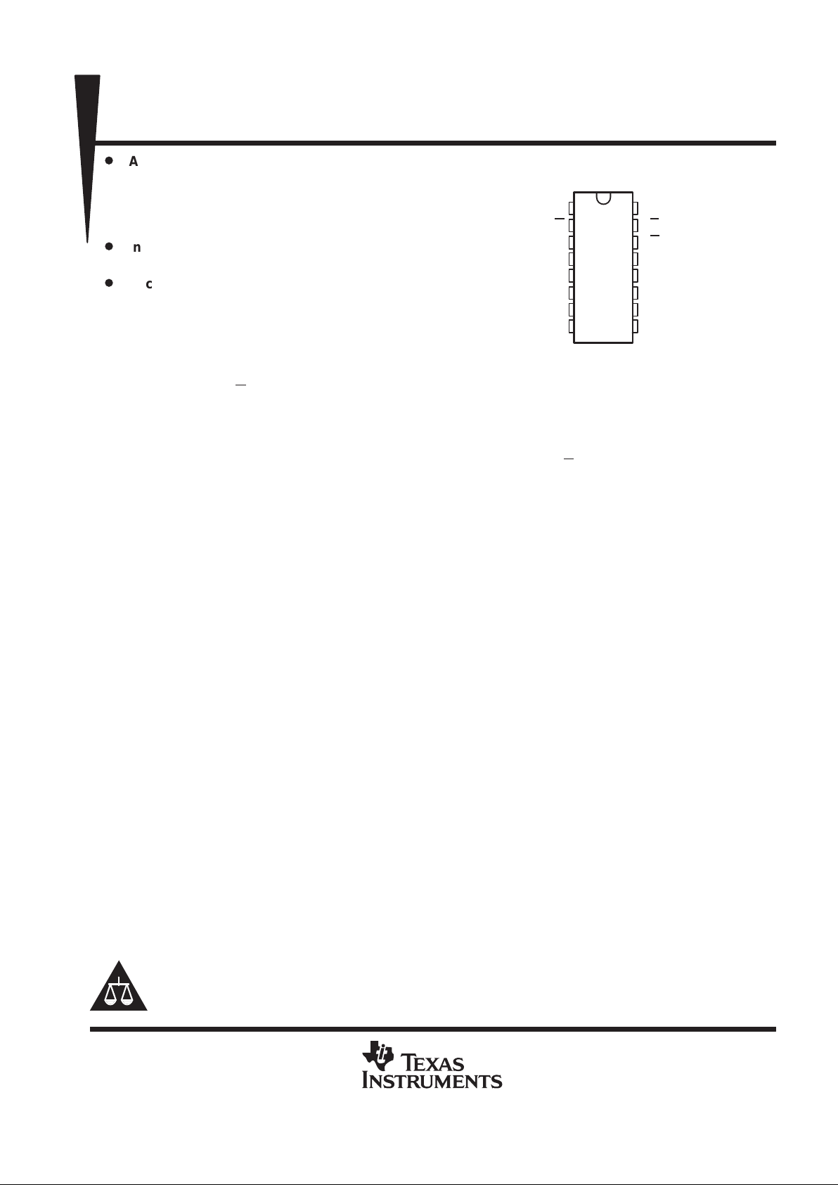
D OR N PACKAGE
(TOP VIEW)
1
2
3
4
5
6
7
8
16
15
14
13
12
11
10
9
1C
1G
B
1Y3
1Y2
1Y1
1Y0
GND
V
CC
2C
2G
A
2Y3
2Y2
2Y1
2Y0
SN74ALS156
DECODER/DEMULTIPLEXER
WITH OPEN-COLLECTOR OUTPUTS
SDAS099C – JUNE 1986 – REVISED MA Y 1996
2
POST OFFICE BOX 655303 • DALLAS, TEXAS 75265
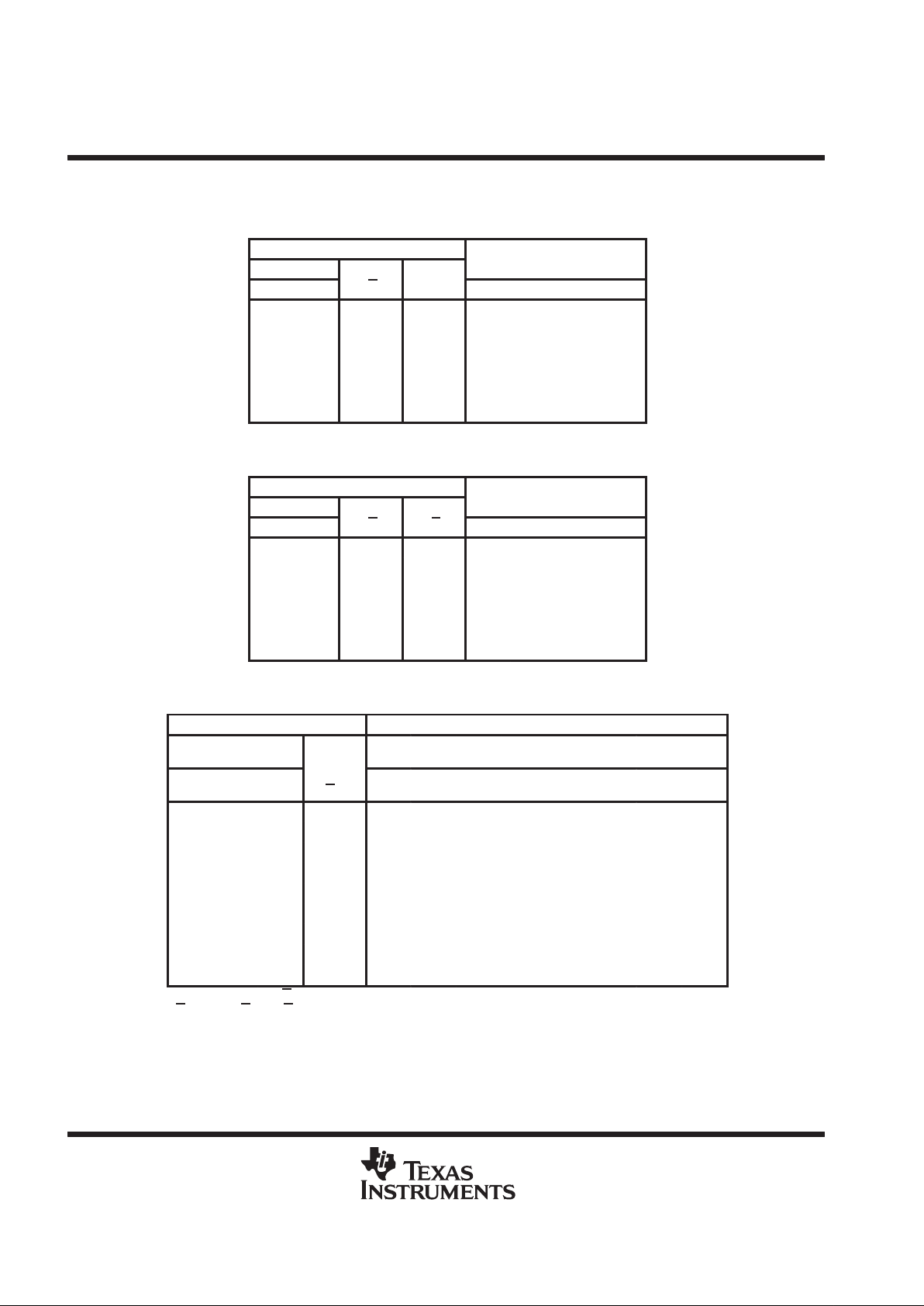
Function Tables
2-LINE TO 4-LINE DECODER OR
1-LINE TO 4-LINE DEMUL TIPLEXER
INPUTS
SELECT
STROBE DATA
OUTPUTS
B A
1G 1C
1Y0 1Y1 1Y2 1Y3
X X H X H H H H
L LL HLHHH
LHL HHLHH
HLL HHHLH
HHL HHHHL
XX X L HHHH
2-LINE TO 4-LINE DECODER OR
1-LINE TO 4-LINE DEMUL TIPLEXER
INPUTS
SELECT
STROBE DATA
OUTPUTS
B A
2G 2C
2Y0 2Y1 2Y2 2Y3
X X H X H H H H
L LL LLHHH
LHL LHLHH
HLL LHHLH
HHL LHHHL
XX X H HHHH
3-LINE TO 8-LINE DECODER OR
1-LINE TO 8-LINE DEMUL TIPLEXER
INPUTS
OUTPUTS
SELECT
STROBE
OR
0 1 2 3 4 5 6 7
C
†
B A
DATA
G
‡
2Y0 2Y1 2Y2 2Y3 1Y0 1Y1 1Y2 1Y3
X X X H H H H H H H H H
L LL L LHHHLHHH
LLH L HLHHHLHH
LHL L HHLHHHHH
LHH L HHHLHHHH
HLL L HHHHLHHH
HLH L HHHHHLHH
HHL L HHLHHHLH
HHH L HHHLHHHL
†
C = inputs 1C and 2C connected together
‡
G
= inputs 1G and 2G connected together
SN74ALS156
DECODER/DEMULTIPLEXER
WITH OPEN-COLLECTOR OUTPUTS
SDAS099C – JUNE 1986 – REVISED MA Y 1996
3
POST OFFICE BOX 655303 • DALLAS, TEXAS 75265
logic symbols† (alternatives)
X/Y
2-LINE TO 4-LINE DECODER
1
1C
4
1Y0
7
1Y1
6
1Y2
5
1Y3
4
0
1
2
3
2Y0
9
2Y1
10
2Y2
11
2Y3
12
0
1
2
3
α
α
α
α
β
β
β
β
2
1
13
A
2
3
B
14
15
&
&
EN
EN
1G
2G
2C
1-LINE TO 4-LINE DEMUL TIPLEXER
0
13
A
1
3
B
G
0
3
DMUX
4
1
1C
G4
2
1G
14
15
2G
2C
1Y0
7
1Y1
6
1Y2
5
1Y3
4
2Y0
9
2Y1
10
2Y2
11
2Y3
12
0
1
2
3
X/Y
3-LINE TO 8-LINE DECODER
C
2Y0
9
2Y1
10
2Y2
11
2Y3
12
0
1
2
3
1Y0
7
1Y1
6
1Y2
5
1Y3
4
4
5
6
7
1
13
A
2
3
B
G
1
15
2
14
EN
2
DMUX
1-LINE TO 8-LINE DEMUL TIPLEXER
C
2Y0
9
2Y1
10
2Y2
11
2Y3
12
0
1
2
3
1Y0
7
1Y1
6
1Y2
5
1Y3
4
4
5
6
7
13
A
3
B
G
1
15
2
14
G
0
7
0
†
These symbols are in accordance with ANSI/IEEE Std 91-1984 and IEC Publication 617-12.

SN74ALS156
DECODER/DEMULTIPLEXER
WITH OPEN-COLLECTOR OUTPUTS
SDAS099C – JUNE 1986 – REVISED MA Y 1996
4
POST OFFICE BOX 655303 • DALLAS, TEXAS 75265
logic diagram (positive logic)
2
1
3
13
15
14
7
6
5
4
9
10
11
12
1Y0
1Y1
1Y2
1Y3
2Y0
2Y1
2Y2
2Y3
Strobe 2G
Strobe 1G
Data 1C
Data 2C
A
B
Select
absolute maximum ratings over operating free-air temperature range (unless otherwise noted)
†
Supply voltage, V
CC
7 V. . . . . . . . . . . . . . . . . . . . . . . . . . . . . . . . . . . . . . . . . . . . . . . . . . . . . . . . . . . . . . . . . . . . . . . .
Input voltage, V
I
7 V. . . . . . . . . . . . . . . . . . . . . . . . . . . . . . . . . . . . . . . . . . . . . . . . . . . . . . . . . . . . . . . . . . . . . . . . . . . .
Operating free-air temperature range, T
A
0°C to 70°C. . . . . . . . . . . . . . . . . . . . . . . . . . . . . . . . . . . . . . . . . . . . . .
Storage temperature range, T
stg
–65°C to 150°C. . . . . . . . . . . . . . . . . . . . . . . . . . . . . . . . . . . . . . . . . . . . . . . . . . .
†
Stresses beyond those listed under “absolute maximum ratings” may cause permanent damage to the device. These are stress ratings only, and
functional operation of the device at these or any other conditions beyond those indicated under “recommended operating conditions” is not
implied. Exposure to absolute-maximum-rated conditions for extended periods may affect device reliability.
recommended operating conditions
MIN NOM MAX UNIT
V
CC
Supply voltage 4.5 5 5.5 V
V
IH
High-level input voltage 2 V
V
IL
Low-level input voltage 0.8 V
V
OH
High-level output voltage 5.5 V
I
OL
Low-level output current 8 mA
T
A
Operating free-air temperature 0 70 °C

SN74ALS156
DECODER/DEMULTIPLEXER
WITH OPEN-COLLECTOR OUTPUTS
SDAS099C – JUNE 1986 – REVISED MA Y 1996
5
POST OFFICE BOX 655303 • DALLAS, TEXAS 75265
electrical characteristics over recommended operating free-air temperature range (unless
otherwise noted)
PARAMETER TEST CONDITIONS MIN TYP†MAX UNIT
V
IK
VCC = 4.5 V, II = –18 mA –1.5 V
IOL = 4 mA 0.25 0.4
VOLV
CC
=
4.5 V
IOL = 8 mA 0.35 0.5
V
I
OH
VCC = 4.5 V, VOH = 5.5 V 0.1 mA
I
I
VCC = 5.5 V, VI = 7 V 0.1 mA
I
IH
VCC = 5.5 V, VI = 2.7 V 20 µA
I
IL
VCC = 5.5 V, VI = 0.4 V –0.1 µA
I
CCL
VCC = 5.5 V 5 9 mA
†
All typical values are at VCC = 5 V, TA = 25°C.
switching characteristics (see Figure 1)
PARAMETER
FROM
(INPUT)
TO
(OUTPUT)
VCC = 4.5 V to 5.5 V,
CL = 50 pF,
RL = 500 Ω
,
TA = MIN to MAX
‡
UNIT
MIN MAX
t
PLH
7 55
t
PHL
A, B
1Y, 2Y
6 25
ns
t
PLH
7 50
t
PHL
1C
1Y
6 23
ns
t
PLH
7 38
t
PHL
1G
1Y
6 22
ns
t
PLH
7 38
t
PHL
2C, 2G
2Y
6 22
ns
‡
For conditions shown as MIN or MAX, use the appropriate value specified under recommended operating conditions.

SN74ALS156
DECODER/DEMULTIPLEXER
WITH OPEN-COLLECTOR OUTPUTS
SDAS099C – JUNE 1986 – REVISED MA Y 1996
6
POST OFFICE BOX 655303 • DALLAS, TEXAS 75265
PARAMETER MEASUREMENT INFORMATION
SERIES 54ALS/74ALS AND 54AS/74AS DEVICES
t
PHZ
t
PLZ
t
PHL
t
PLH
0.3 V
t
PZL
t
PZH
t
PLH
t
PHL
LOAD CIRCUIT
FOR 3-STATE OUTPUTS
From Output
Under Test
Test
Point
R1
S1
C
L
(see Note A)
7 V
1.3 V
1.3 V1.3 V
3.5 V
3.5 V
0.3 V
0.3 V
t
h
t
su
VOLTAGE WAVEFORMS
SETUP AND HOLD TIMES
Timing
Input
Data
Input
1.3 V 1.3 V
3.5 V
3.5 V
0.3 V
0.3 V
High-Level
Pulse
Low-Level
Pulse
t
w
VOLTAGE WAVEFORMS
PULSE DURATIONS
Input
Out-of-Phase
Output
(see Note C)
1.3 V 1.3 V
1.3 V1.3 V
1.3 V 1.3 V
1.3 V1.3 V
1.3 V
1.3 V
3.5 V
3.5 V
0.3 V
0.3 V
V
OL
V
OH
V
OH
V
OL
Output
Control
(low-level
enabling)
Waveform 1
S1 Closed
(see Note B)
Waveform 2
S1 Open
(see Note B)
[
0 V
V
OH
V
OL
[
3.5 V
In-Phase
Output
0.3 V
1.3 V 1.3 V
VOLTAGE WAVEFORMS
PROPAGATION DELAY TIMES
VOLTAGE WAVEFORMS
ENABLE AND DISABLE TIMES, 3-STATE OUTPUTS
R2
V
CC
R
L
Test
Point
From Output
Under Test
C
L
(see Note A)
LOAD CIRCUIT
FOR OPEN-COLLECTOR OUTPUTS
LOAD CIRCUIT FOR
BI-STATE
TOTEM-POLE OUTPUTS
From Output
Under Test
Test
Point
C
L
(see Note A)
R
L
RL = R1 = R2
NOTES: A. CL includes probe and jig capacitance.
B. Waveform 1 is for an output with internal conditions such that the output is low except when disabled by the output control.
Waveform 2 is for an output with internal conditions such that the output is high except when disabled by the output control.
C. When measuring propagation delay items of 3-state outputs, switch S1 is open.
D. All input pulses have the following characteristics: PRR ≤ 1 MHz, tr = tf = 2 ns, duty cycle = 50%.
E. The outputs are measured one at a time with one transition per measurement.
Figure 1. Load Circuits and Voltage Waveforms

IMPORTANT NOTICE
T exas Instruments and its subsidiaries (TI) reserve the right to make changes to their products or to discontinue
any product or service without notice, and advise customers to obtain the latest version of relevant information
to verify, before placing orders, that information being relied on is current and complete. All products are sold
subject to the terms and conditions of sale supplied at the time of order acknowledgement, including those
pertaining to warranty, patent infringement, and limitation of liability.
TI warrants performance of its semiconductor products to the specifications applicable at the time of sale in
accordance with TI’s standard warranty. Testing and other quality control techniques are utilized to the extent
TI deems necessary to support this warranty. Specific testing of all parameters of each device is not necessarily
performed, except those mandated by government requirements.
CERT AIN APPLICATIONS USING SEMICONDUCTOR PRODUCTS MAY INVOLVE POTENTIAL RISKS OF
DEATH, PERSONAL INJURY, OR SEVERE PROPERTY OR ENVIRONMENTAL DAMAGE (“CRITICAL
APPLICATIONS”). TI SEMICONDUCTOR PRODUCTS ARE NOT DESIGNED, AUTHORIZED, OR
WARRANTED TO BE SUITABLE FOR USE IN LIFE-SUPPORT DEVICES OR SYSTEMS OR OTHER
CRITICAL APPLICATIONS. INCLUSION OF TI PRODUCTS IN SUCH APPLICA TIONS IS UNDERST OOD TO
BE FULLY AT THE CUSTOMER’S RISK.
In order to minimize risks associated with the customer’s applications, adequate design and operating
safeguards must be provided by the customer to minimize inherent or procedural hazards.
TI assumes no liability for applications assistance or customer product design. TI does not warrant or represent
that any license, either express or implied, is granted under any patent right, copyright, mask work right, or other
intellectual property right of TI covering or relating to any combination, machine, or process in which such
semiconductor products or services might be or are used. TI’s publication of information regarding any third
party’s products or services does not constitute TI’s approval, warranty or endorsement thereof.
Copyright 1998, Texas Instruments Incorporated
 Loading...