

Texas Instruments SN74ALB16244DGGR, SN74ALB16244DGVR, SN74ALB16244DL, SN74ALB16244DLR Datasheet
SN74ALB16244
16-BIT BUFFER/DRIVER
WITH 3-STATE OUTPUTS
SCBS647C – AUGUST 1995 – REVISED JUL Y 1997
D
Member of the Texas Instruments
Widebus
D
State-of-the-Art Advanced Low-Voltage
Family
BiCMOS (ALB) Technology Design for 3.3-V
Operation
D
Schottky Diodes on All Inputs to Eliminate
Overshoot and Undershoot
D
Industry Standard ’16244 Pinout
D
Distributed VCC and GND Pin Configuration
Minimizes High-Speed Switching Noise
D
Flow-Through Architecture Optimizes PCB
Layout
D
Package Options Include Plastic 300-mil
Shrink Small-Outline (DL) and Thin Shrink
Small-Outline (DGG) Packages
description
The SN74ALB16244 16-bit buffer and line driver
is designed for high-speed, low-voltage (3.3-V)
V
operation. This device is intended to replace
CC
the conventional driver in any speed-critical path.
The small propagation delay is achieved using a
unity gain amplifier on the input and feedback
resistors from input to output, which allows the
output to track the input with a small offset voltage.
The device can be used as four 4-bit buffers, two
8-bit buffers, or one 16-bit buffer. This device
provides true outputs and symmetrical active-low
output-enable (OE
) inputs.
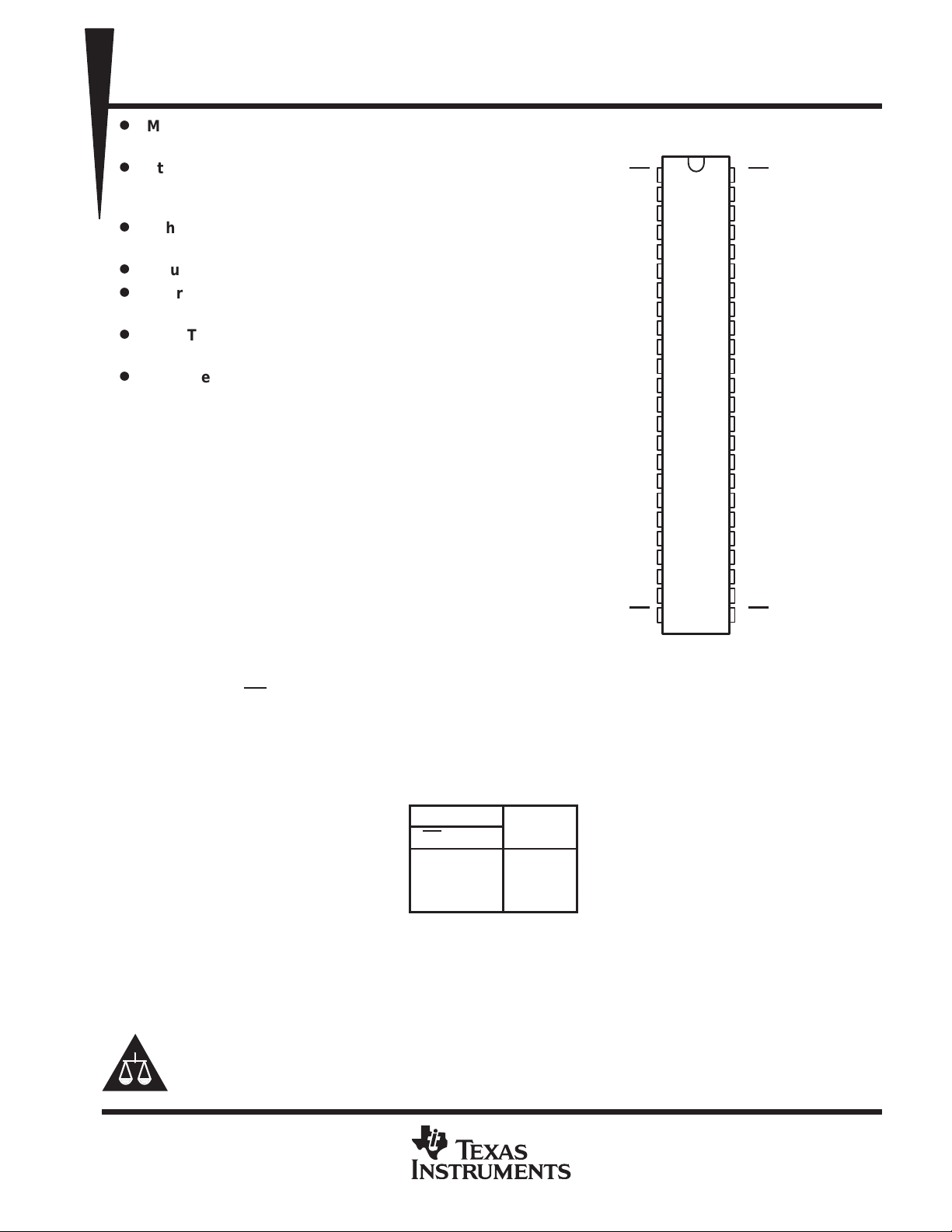
DGG OR DL PACKAGE
(TOP VIEW)
1OE
1
48
1Y1
2
47
1Y2
3
46
GND
GND
GND
GND
1Y3
1Y4
V
CC
2Y1
2Y2
2Y3
2Y4
3Y1
3Y2
3Y3
3Y4
V
CC
4Y1
4Y2
4Y3
4Y4
4OE
4
5
6
7
8
9
10
11
12
13
14
15
16
17
18
19
20
21
22
23
24
45
44
43
42
41
40
39
38
37
36
35
34
33
32
31
30
29
28
27
26
25
2OE
1A1
1A2
GND
1A3
1A4
V
CC
2A1
2A2
GND
2A3
2A4
3A1
3A2
GND
3A3
3A4
V
CC
4A1
4A2
GND
4A3
4A4
3OE
The SN74ALB16244 is characterized for
operation from –40°C to 85°C.
Please be aware that an important notice concerning availability, standard warranty, and use in critical applications of
Texas Instruments semiconductor products and disclaimers thereto appears at the end of this data sheet.
Widebus is a trademark of Texas Instruments Incorporated.
PRODUCTION DATA information is current as of publication date.
Products conform to specifications per the terms of Texas Instruments
standard warranty. Production processing does not necessarily include
testing of all parameters.
FUNCTION TABLE
(each buffer)
INPUTS
OE
L H H
L LL
H X Z
OUTPUT
A
Y
Copyright 1997, Texas Instruments Incorporated
POST OFFICE BOX 655303 • DALLAS, TEXAS 75265
1

SN74ALB16244
16-BIT BUFFER/DRIVER
WITH 3-STATE OUTPUTS
SCBS647C – AUGUST 1995 – REVISED JUL Y 1997
logic symbol
†
1A1
1A2
1A3
1A4
2A1
2A2
2A3
2A4
3A1
3A2
3A3
3A4
4A1
4A2
4A3
4A4
1
48
25
24
47
46
44
43
41
40
38
37
36
35
33
32
30
29
27
26
EN1
EN2
EN3
EN4
11
12
13
14
16
17
19
20
22
23
2
1Y1
3
1Y2
5
1Y3
6
1Y4
8
2Y1
9
2Y2
2Y3
2Y4
3Y1
3Y2
3Y3
3Y4
4Y1
4Y2
4Y3
4Y4
1
1
1
2
1
3
1
4
1OE
2OE
3OE
4OE
†
This symbol is in accordance with ANSI/IEEE Std 91-1984 and IEC Publication 617-12.
2
POST OFFICE BOX 655303 • DALLAS, TEXAS 75265
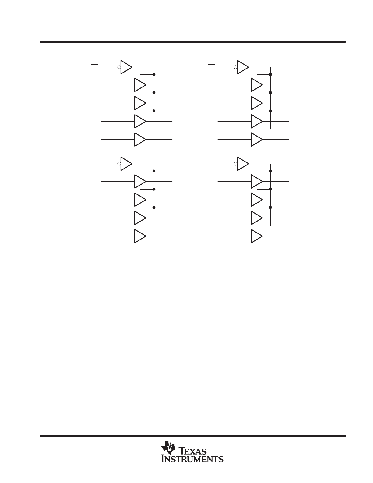
logic diagram (positive logic)
SN74ALB16244
16-BIT BUFFER/DRIVER
WITH 3-STATE OUTPUTS
SCBS647C – AUGUST 1995 – REVISED JUL Y 1997
1OE
1A1
1A2
1A3
1A4
2OE
2A1
2A2
2A3
2A4
1
47
46
44
43
48
41
40
38
37
11
12
25
3OE
2
1Y1
3
1Y2
5
1Y3
6
1Y4
8
2Y1
9
2Y2
2Y3
2Y4
3A1
3A2
3A3
3A4
4OE
4A1
4A2
4A3
4A4
36
35
33
32
24
30
29
27
26
13
14
16
17
19
20
22
23
3Y1
3Y2
3Y3
3Y4
4Y1
4Y2
4Y3
4Y4
absolute maximum ratings over operating free-air temperature range (unless otherwise noted)
Supply voltage range, VCC –0.5 V to 4.6 V. . . . . . . . . . . . . . . . . . . . . . . . . . . . . . . . . . . . . . . . . . . . . . . . . . . . . . . . .
Input voltage range, VI: Except I/O ports (see Note 1) –0.5 V to 4.6 V. . . . . . . . . . . . . . . . . . . . . . . . . . . . . . . . .
I/O ports (see Notes 1 and 2) –0.5 V to VCC + 0.5 V. . . . . . . . . . . . . . . . . . . . . . . . . . .
Output voltage range, VO (see Notes 1 and 2) –0.5 V to VCC + 0.5 V. . . . . . . . . . . . . . . . . . . . . . . . . . . . . . . . . .
Input clamp current, I
Output clamp current, I
Continuous output current, I
Continuous current through each V
Package thermal impedance, θ
Storage temperature range, T
†
Stresses beyond those listed under “absolute maximum ratings” may cause permanent damage to the device. These are stress ratings only, and
functional operation of the device at these or any other conditions beyond those indicated under “recommended operating conditions” is not
implied. Exposure to absolute-maximum-rated conditions for extended periods may affect device reliability.
NOTES: 1. The input and output negative-voltage ratings may be exceeded if the input and output clamp-current ratings are observed.
2. This value is limited to 4.6 V maximum.
3. The package thermal impedance is calculated in accordance with JESD 51.
(V
< 0) –50 mA. . . . . . . . . . . . . . . . . . . . . . . . . . . . . . . . . . . . . . . . . . . . . . . . . . . . . . . . . . .
IK
I
(V
OK
< 0 or VO > VCC) ±50 mA. . . . . . . . . . . . . . . . . . . . . . . . . . . . . . . . . . . . . . . . . . . .
O
(V
= 0 to VCC) ±50 mA. . . . . . . . . . . . . . . . . . . . . . . . . . . . . . . . . . . . . . . . . . . . . .
O
O
or GND ±100 mA. . . . . . . . . . . . . . . . . . . . . . . . . . . . . . . . . . . . . . . . . . . . .
CC
(see Note 3): DGG package 89°C/W. . . . . . . . . . . . . . . . . . . . . . . . . . . . . . .
JA
DL package 94°C/W. . . . . . . . . . . . . . . . . . . . . . . . . . . . . . . . .
–65°C to 150°C. . . . . . . . . . . . . . . . . . . . . . . . . . . . . . . . . . . . . . . . . . . . . . . . . . .
stg
†
POST OFFICE BOX 655303 • DALLAS, TEXAS 75265
3
 Loading...