

SN74AHCT1G125
SINGLE BUS BUFFER GATE
WITH 3-STATE OUTPUT
SCLS378F – AUGUST 1997 – REVISED JANUARY 2000
D
EPIC
(Enhanced-Performance Implanted
CMOS) Process
D
Inputs Are TTL-Voltage Compatible
D
Latch-Up Performance Exceeds 250 mA Per
JESD 17
D
Package Options Include Plastic
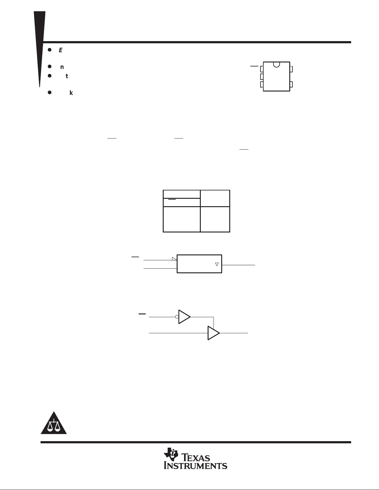
DBV OR DCK PACKAGE
(TOP VIEW)
OE
GND
1
A
2
3
V
5
Y
4
CC
Small-Outlline Transistor (DBV, DCK)
Packages
description
The SN74AHCT1G125 is a single bus buffer gate/line driver with 3-state output. The output is disabled when
the output-enable (OE
T o ensure the high-impedance state during power up or power down, OE
resistor; the minimum value of the resistor is determined by the current-sinking capability of the driver.
The SN74AHCT1G125 is characterized for operation from –40°C to 85°C.
) input is high. When OE is low, true data is passed from the A input to the Y output.
should be tied to VCC through a pullup
FUNCTION TABLE
INPUTS
OE A
L H H
L LL
H X Z
OUTPUT
Y
logic symbol
†
This symbol is in accordance with ANSI/IEEE Std 91-1984 and IEC Publication 617-12.
†
1
OE
2
A
EN
logic diagram (positive logic)
1
OE
24
AY
Please be aware that an important notice concerning availability, standard warranty, and use in critical applications of
Texas Instruments semiconductor products and disclaimers thereto appears at the end of this data sheet.
4
Y
EPIC is a trademark of Texas Instruments Incorporated.
PRODUCTION DATA information is current as of publication date.
Products conform to specifications per the terms of Texas Instruments
standard warranty. Production processing does not necessarily include
testing of all parameters.
POST OFFICE BOX 655303 • DALLAS, TEXAS 75265
Copyright 2000, Texas Instruments Incorporated
1
SN74AHCT1G125
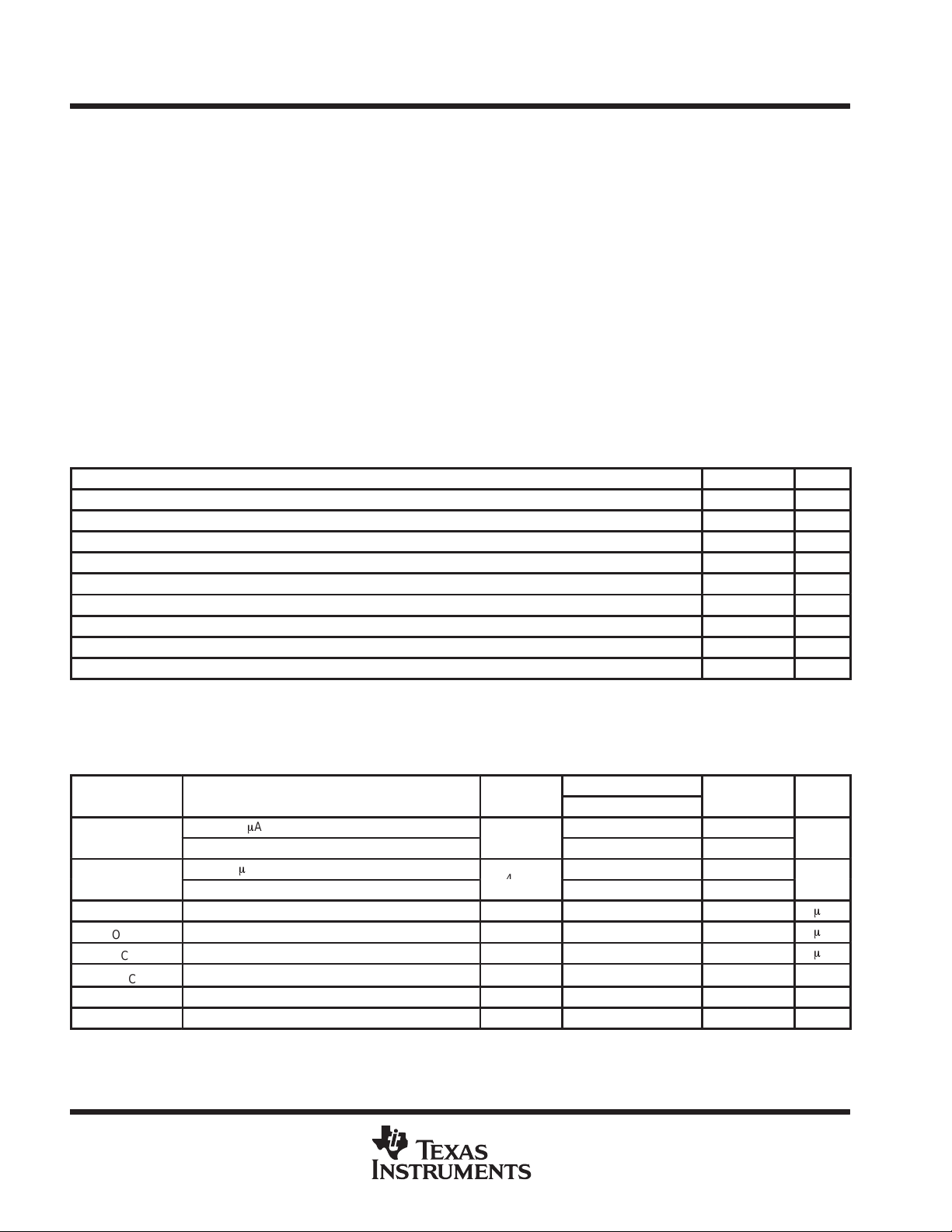
PARAMETER
TEST CONDITIONS
V
MIN
MAX
UNIT
V
4.5 V
V
V
4.5 V
V
SINGLE BUS BUFFER GATE
WITH 3-STATE OUTPUT
SCLS378F – AUGUST 1997 – REVISED JANUARY 2000
absolute maximum ratings over operating free-air temperature range (unless otherwise noted)
†
Supply voltage range, VCC –0.5 V to 7 V. . . . . . . . . . . . . . . . . . . . . . . . . . . . . . . . . . . . . . . . . . . . . . . . . . . . . . . . . .
Input voltage range, VI (see Note 1) –0.5 V to 7 V. . . . . . . . . . . . . . . . . . . . . . . . . . . . . . . . . . . . . . . . . . . . . . . . . .
Output voltage range, V
Input clamp current, I
Output clamp current, I
(see Note 1) –0.5 V to V
O
(V
IK
I
OK
Continuous output current, I
< 0) –20 mA. . . . . . . . . . . . . . . . . . . . . . . . . . . . . . . . . . . . . . . . . . . . . . . . . . . . . . . . . . .
(V
< 0 or VO > VCC) ±20 mA. . . . . . . . . . . . . . . . . . . . . . . . . . . . . . . . . . . . . . . . . . . .
O
(V
= 0 to VCC) ±25 mA. . . . . . . . . . . . . . . . . . . . . . . . . . . . . . . . . . . . . . . . . . . . . .
O
O
CC
+ 0.5 V. . . . . . . . . . . . . . . . . . . . . . . . . . . . . . . . . . . . . . . .
Continuous current through VCC or GND ±50 mA. . . . . . . . . . . . . . . . . . . . . . . . . . . . . . . . . . . . . . . . . . . . . . . . . . .
Package thermal impedance, θ
(see Note 2): DBV package 347°C/W. . . . . . . . . . . . . . . . . . . . . . . . . . . . . . .
JA
DCK package 389°C/W. . . . . . . . . . . . . . . . . . . . . . . . . . . . . . .
Storage temperature range, T
†
Stresses beyond those listed under “absolute maximum ratings” may cause permanent damage to the device. These are stress ratings only, and
functional operation of the device at these or any other conditions beyond those indicated under “recommended operating conditions” is not
implied. Exposure to absolute-maximum-rated conditions for extended periods may affect device reliability.
NOTES: 1. The input and output voltage ratings may be exceeded if the input and output current ratings are observed.
2. The package thermal impedance is calculated in accordance with JESD 51.
–65°C to 150°C. . . . . . . . . . . . . . . . . . . . . . . . . . . . . . . . . . . . . . . . . . . . . . . . . . .
stg
recommended operating conditions (see Note 3)
MIN MAX UNIT
V
V
V
V
V
I
OH
I
OL
∆t/∆v Input transition rise or fall rate 20 ns/V
T
NOTE 3: All unused inputs of the device must be held at VCC or GND to ensure proper device operation. Refer to the TI application report,
Supply voltage 4.5 5.5 V
CC
High-level input voltage 2 V
IH
Low-level input voltage 0.8 V
IL
Input voltage 0 5.5 V
I
Output voltage 0 V
O
High-level output current –8 mA
Low-level output current 8 mA
Operating free-air temperature –40 85 °C
A
Implications of Slow or Floating CMOS Inputs
, literature number SCBA004.
CC
V
electrical characteristics over recommended operating free-air temperature range (unless
otherwise noted)
‡
2
CC
OH
OL
I
I
I
OZ
I
CC
‡
∆I
CC
C
i
C
o
This is the increase in supply current for each input at one of the specified TTL voltage levels rather than 0 V or VCC.
IOH = –50 mA
IOH = –8 mA
IOL = 50 mA
IOL = 8 mA
VI = VCC or GND 0 V to 5.5 V ±0.1 ±1
VO = VCC or GND 5.5 V ±0.25 ±2.5
VI = VCC or GND, IO = 0 5.5 V 1 10
One input at 3.4 V , Other input at VCC or GND 5.5 V 1.35 1.5 mA
VI = VCC or GND 5 V 4 10 10 pF
VO = VCC or GND 5 V 10 pF
POST OFFICE BOX 655303 • DALLAS, TEXAS 75265
TA = 25°C
MIN TYP MAX
4.4 4.5 4.4
3.94 3.8
0.1 0.1
0.36 0.44
m
A
m
A
m
A
 Loading...